A few months ago, Terasic unveiled its SoCKit powered by Altera Cyclone V dual Cortex A9 + FPGA. They’ve now announced a cheaper version will a less powerful Cyclone V SoC and lower specs (e.g. less RAM, only one sensor, etc…) that sells for as low as $150 for educational or academic purposes, and $199 for the rest of us.
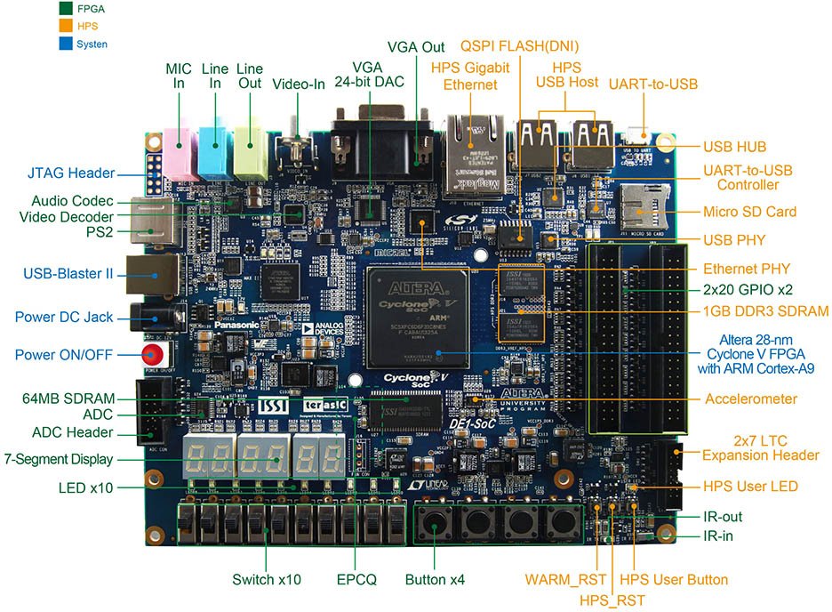
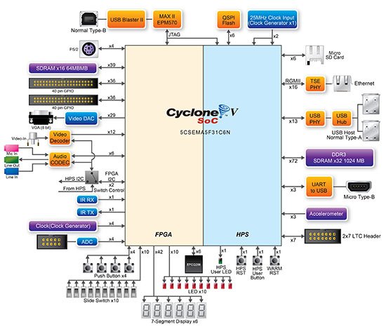
Altera DE1-SoC Board specifications:
- FPGA Device
- Cyclone V SoC 5CSEMA5F31 Device
- Dual-core ARM Cortex-A9 (HPS – Hard Processor System)
- 85K Programmable Logic Elements
- 4,450 Kbits embedded memory
- 6 Fractional PLLs
- 2 Hard Memory Controllers
- Configuration and Debug
- Quad Serial Configuration device – EPCQ256 on FPGA (EPCQ = Erasable Programmable Configurable Quad-SPI device)
- On-Board USB Blaster II (Normal type B USB connector)
- Memory Device
- 64MB (32Mx16) SDRAM on FPGA
- 1GB (2x256Mx16) DDR3 SDRAM on HPS
- 128MB QSPI Flash on HPS (QSPI Flash does not come pre-installed out of factory)
- Micro SD Card Socket on HPS
- Communication
- Two Port USB 2.0 Host (ULPI interface with USB type A connector)
- USB to UART (micro USB type B connector)
- 10/100/1000 Ethernet
- PS/2 mouse/keyboard
- IR Emitter/Receiver
- Connectors
- Two 40-pin Expansion Headers
- One 10-pin ADC Input Header
- One LTC connector (One Serial Peripheral Interface (SPI) Master ,one I2C and one GPIO interface )
- Display – 24-bit VGA DAC
- Audio – 24-bit CODEC, Line-in, line-out, and microphone-in jacks
- Video Input – TV Decoder (NTSC/PAL/SECAM) and TV-in connector
- Switches, Buttons and Indicators
- 4 User Keys (FPGA x4)
- 10 User switches (FPGA x10)
- 11 User LEDs (FPGA x10 ; HPS x 1)
- 2 HPS Reset Buttons (HPS_RST_n and HPS_WARM_RST_n)
- Six 7-segment displays
- Sensors – G-Sensor on HPS
- Power – 12V DC input
- Dimensions – 166×130 mm
The DE1-SOC Development Kit contains the board, a Quick Start Guide, DE1-SoC System CD-ROM, a 12V power adapter, a type A to micro B USB cable, and a type A to B USB cable. The company claims you’ll need a computer that runs Microsoft Windows XP or later in order to use the tools, but Quartus II, one of the tools, appears to be available for both Windows and Linux.
The video below provides an introduction, then show a demo with DE1-SoC board (video + audio), and explains how the FPGA works in the demo.

Further information is available on Terasic’s Altera DE1-SoC page, and in due time, the board will probably be listed on Altera University Program site where you’ll be able to purchase the board and download documentations. Note: There’s already a DE1 board, but this is a different hardware based on Cyclone II FPGA.

Jean-Luc started CNX Software in 2010 as a part-time endeavor, before quitting his job as a software engineering manager, and starting to write daily news, and reviews full time later in 2011.
Support CNX Software! Donate via cryptocurrencies, become a Patron on Patreon, or purchase goods on Amazon or Aliexpress
Sort of idiotic to have a video that comes up “This video is private.” Oh well, idiots abound.
@LJR
Looks like Terasic changes the settings for their video, not sure why.
Maybe replaced by that one: http://www.youtube.com/watch?v=aPXMkTJxD_s
goob