UCIe (Universal Chiplet Interconnect Express) open standard for Chiplets with heterogeneous chips

UCIe Open Chiplet platform-on-a-package

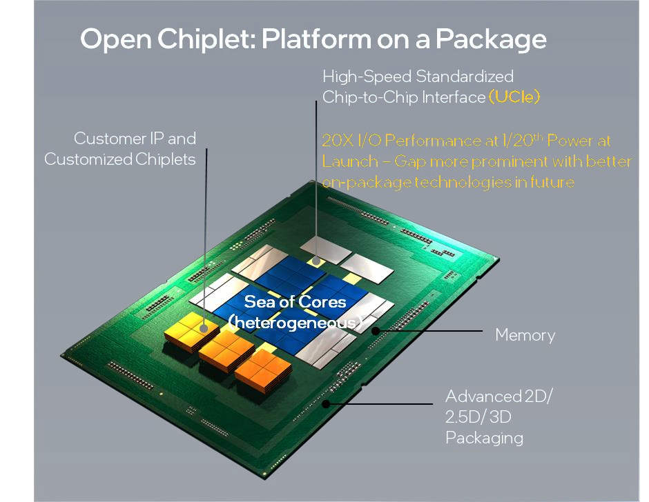
We first heard about Chiplet, chips that gather IP or chips from different vendors into a single chip, in 2020 with the now-defunct zGlue’s Open Chiplet Initiative, but the term recently came back to the forefront last month with Intel’s investment into the “Open Chiplet Platform” that aims to offer a modular approach to chip design through chiplets with each block/chiplet customized for a particular function. It turns out there’s now an official standard called the Universal Chiplet Interconnect Express (UCIe) whose specification defines the interconnect between chiplets within a package, and not only backed by Intel, but also AMD, Arm, ASE, Google Cloud, Meta, Microsoft, Qualcomm, Samsung, and TSMC. UCIe defines the Physical Layer (Die-to-Die I/O) and protocols to be used for the chiplet interfaces, currently PCIe and CXL (Compute Express Link), but more protocols will be added to the specification in the future. The goal is to provide […]

Intel launches Alder Lake P-Series and U-Series mobile hybrid processors

Intel-Alder Lake P-Series and U-Series block diagram

Intel first unveiled the most powerful Alder Lake H-Series last year before the launch in January, and also introduced Alder Lake-S desktop IoT processors and Alder Lake U-Series and P-Series mobile IoT SoCs in early January. But now the company has announced the launch of the Alder Lake P-Series (28W) and U-Series (9W and 15 PBP) 12th generation mobile processors designed for “thin-and-light” laptops which should become available around March 2022. The block diagram of the 28W P-Series and 15W U-Series (source: product brief from Intel) shows both offer the same interfaces including eDP 1.4b, HDMI 2.0b, 2x PCIe Gen4, 12x PCIe Gen3, 2x SATA… and the same 50x25x12mm BGA package. But the 9W U-Series comes in a cost-optimized 28.5x19x11mm BGA package that does without SATA interfaces, a lower number of PCIe Gen3 interfaces (10 vs 12), USB 2.0 interfaces (6 vs 10), Thunderbolt 4 interfaces (2 vs 4), and […]

Intel aims to be the performance per watt leader by 2024 with Lunar Lake processors

Intel Roadmap to 2024 and beyond

Apple-designed Arm processors have shown it’s possible to get high-performance at relatively low power, and this has left competitors behind in that regard. But Intel aims to rectify that with the goal of becoming the “performance per watt leader” by 2024 with the new Lunar Lake processors manufactured with Intel 18A process. Intel also provided some details about families following Alder Lake processors with Raptor Lake expected later this year, Meteor Lake and Arrow Lake based on Intel 4 and 20A processes in 2023-2024 2022, and Lunar Lake expected in 2024+. Let’s have a look at what we know so far for each family. Intel Raptor Lake The Raptor Lake processors will rely on the same “Intel 7” process as Alder Lake processors, offer up to double-digit performance boost (translation: up to around 10% in specific workloads), up to 24 cores and 32-threads, better overclocking, support for AI M.2 modules […]

Intel to invest $1 billion in foundry innovation, becomes RISC-V International member

Intel RISC-V

Intel has just announced a $1 billion fund to support companies bringing innovations and new technologies to the foundry ecosystem. The company says the fund will prioritize investments in “capabilities that accelerate foundry customers’ time to market – spanning intellectual property (IP), software tools, innovative chip architectures, and advanced packaging technologies.” What’s interesting is that it does not only cover x86 architecture but also Arm and RISC-V, with a focus on the latter, as Intel has just become a Premier member of RISC-V International, and partnered with several companies offering RISC-V solutions including Andes Technology, Esperanto Technologies, SiFive, and Ventana Micro Systems. Intel’s Open Chiplet Platform Part of the investment will go to the Open Chiplet Platform offering a modular approach to chip design through chiplets with each block/chiplet customized for a particular function. This will allow designers to select the best IP and process technologies for a particular SoC. […]

Intel launches NUC 11 Essential mini PC, Kits, and SBC with Jasper Lake SoC

Intel NUC 11 Essential

Details about the Intel NUC 11 Essential “Atlas Canyon” mini PCs with Jasper Lake processor were leaked in May 2021, but Intel has now made it official with the “launch” of five NUC 11 Essential SKUs with one Windows 11 mini PC with 4GB RAM and 64GB storage, three kits (bare mini PC), and one bare board all listed on Ark Intel. I put “launch” between quotes because it’s only “launched” as stated on Ark Intel, but it does not look like it’s available for sale just yet, but now at least we get confirmation about the specs from the leak that was fairly accurate, except Intel did not launch 10W Jasper Lake J-Series processors, and both 6W and 10W Jasper Lake processors are part of the N-Series. Intel NUC 11 Essential specifications: SoC/memory/storage NUC11ATKC2 Mini PC SoC – Intel Celeron N4505 dual-core processor clocked at 2.0 GHz / 2.9 […]

TDP (Thermal Design Power) vs PBP (Processor Base Power) – Are there differences?

TDP (Thermal Design Power) metric has been used for years to help manufacturers design appropriate cooling solutions for Intel/AMD processors and give an idea of their power consumption. But I did not immediately catch up that TDP was gone from the recent Alder Lake IoT processors announcement, and Intel is now using PBP (Processor Base Power) instead, while somehow cTDP (configurable TDP) down/up numbers are still provided. Beyond the announcement, if we look into the Intel Ark database, older processors still show TDP, while it’s completely gone for new processors with the specs instead listing Processor Base Power (PBP), and for the ones with Turbo mode “Maximum Turbo Power” (MTP) is also included. But what do those mean exactly? Intel “explains”: TDP definition: Thermal Design Power (TDP) represents the average power, in watts, the processor dissipates when operating at Base Frequency with all cores active under an Intel-defined, high-complexity workload. […]

Intel Mobileye EyeQ Ultra RISC-V processor targets Level 4 autonomous driving

Mobileye EyeQ Ultra

Let’s carry on with Intel’s CES 2022 news, but with a twist as Mobileye EyeQ Ultra does not include any x86 cores, but instead, the automotive processor features 12 RISC-V cores, Arm GPU and DSP, and aims to bring Level 4 autonomous driving to cars thanks notably to a 176 TOPS AI accelerator. The company says EyeQ Ultra packs the performance of 10 EyeQ5s in a single package, with the single chip solution avoiding the power consumption and costs related to integrating multiple SoCs together.   Intel Mobileye EyeQ Ultra specifications highlights: CPU – 12 RISC-V CPU cores  (24 threads) GPU – Unnamed Arm GPU DSP – Unnamed Arm DSP SIMD cores VLIW cores Coarse grained reconfigurable array (CGRA) cores CNN accelerator clusters Two sensing subsystems One camera-only system Radar and Lidar combined system 5-nanometer process technology Mobileye provides both the chip and software with for instance high-definition map and […]

Intel unveils Alder Lake desktop and mobile IoT processors

Intel Alder Lake-H Mobile IoT processsor

Intel introduced high-end Alder Lake Hybrid processor family for consumer devices a couple of months ago, with Pentium G7400 and Celeron G6900 leaking a few weeks later, and now the company has formally announced the Alder Lake-S and Alder Lake-H processor families for respectively desktop IoT and mobile IoT solutions, as well as more efficient U-series and P-series of 12th Gen Intel Core Alder Lake IoT processors with a TDP ranging from 15W to 28W. Alder Lake S-Series desktop processors for IoT Key features and specifications: CPU Up to 16 cores, up to 24 threads in IoT SKUs Up to 30 MB Intel Smart Cache TDP – 35W to 65W Real-time capability on select SKUs Graphics/Video Intel UHD Graphics 770 driven by Intel Xe architecture with up to 32 EUs Up to four independent displays up to 4K or one display at 8K resolution Up to two video decode boxes […]