Lattice Semiconductor has recently introduced the MachXO5D-NX FPGA family, which integrates a hardware root of trust (RoT) into low-power FPGAs. This addresses security challenges by combining on-chip Flash memory and hardware encryption to minimize code capture risks during load time. The MachXO5D-NX family includes three variants with logic cell counts of 27k (FMXO5-25), 53k (LFMXO5-55T), and 96k (LFMXO5-100T). These FPGAs feature built-in hardware encryption, a cryptographic engine supporting AES-256, ECDSA-384/521, SHA2-256/384/512, and RSA 3072/4096, and a unique secret identity (USID) for device identity protection. Built on a 28-nm fully-depleted silicon-on-insulator (FD-SOI) process, these FPGAs reduce power consumption by 75% and lower soft error rates by 100x(as the company mentions). They support interfaces such as MIPI D-PHY (CSI-2, DSI), LVDS, Gigabit Ethernet, and PCIe, making them suitable for secure edge applications. Lattice MachXO5D-NX FPGA family specifications FPGA – Lattice Semi MachXO5D-NX FPGA family (27k (FMXO5-25), 53k (LFMXO5-55T), and 96k (LFMXO5-100T)) Programmable […]
Lattice Semi Certus-NX-09 and Certus-NX-28 small footprint, low-power FPGAs feature optional PCIe Gen2 interface
Lattice Semiconductor has added two new devices to its small, low-power Lattice Certus-NX FPGA family, namely the Certus-NX-28 and Certus-NX-09 available in multiple packages and designed for communications, computing, industrial, and automotive applications. The Certus-NX FPGAs enable power-efficient PCIe Gen 2 with up to 4 times lower power compared to other FPGAs, and ultra-small form factor with up to 2 times more I/O per mm2 and PCIe and Gigabit Ethernet implementation in packages as small as 36 mm2. The company also claims high reliability and security with up to 100 times lower soft error rate, built-in SEC (Soft Error Correction) and memory block ECC for SEU (Single-Even Upset) protection, and up to 12 times faster instant-on configuration performance. The Lattice Certus-NX family is now comprised of four SKUs: LFD2NX-9, LFD2NX-17, LFD2NX-28, and LFD2NX-40 whose main highlights are shown in the comparison table below. The Certus-NX are available in various packages […]
Lattice FeatherWing – An iCE40-powered add-on FPGA board for Adafruit Feather
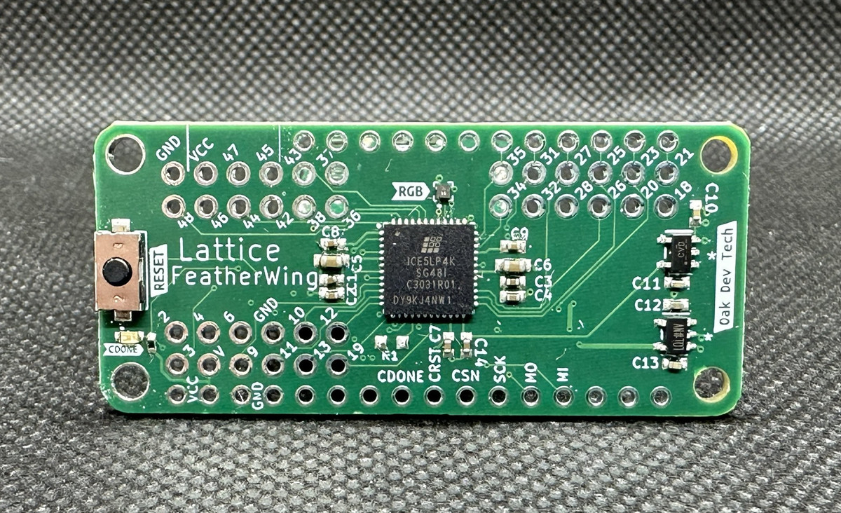
Oak Development Technologies has recently announced Lattice FeatherWing – An iCE40-based development board designed to be controlled by Adafruit Feather. Previously we wrote about the IcyBlue Feather V2, a standalone development built around a Lattice Semi iCE5LP4K FPGA. But this FeatherWing board is designed to add functionality to your existing Adafruit Feather board. The Lattice FeatherWing expands your Adafruit Feather with a Lattice iCE5LP4K FPGA. It connects and gets programmed over SPI so you can use all the FPGA’s GPIO pins through the header blocks. There’s also a built-in RGB LED directly connected to the FPGA’s open-drain pins, for visual feedback. Previously, we have written about many Lattice Semi FPGA-based development boards, such as the tinyVision.ai Pico-Ice board, Silicon Witchery S1, and ULX3S Education Board. Feel free to check those out if you want a standalone FPGA board. FPGA – Lattice Semi iCE40 Family ICE5LP4K-SG48ITR Logic Cells – Approximately 3520 logic cells Memory – 80 Kbits […]
NRFICE is a Bluetooth FPGA board in the Arduino UNO form factor (Crowdfunding)
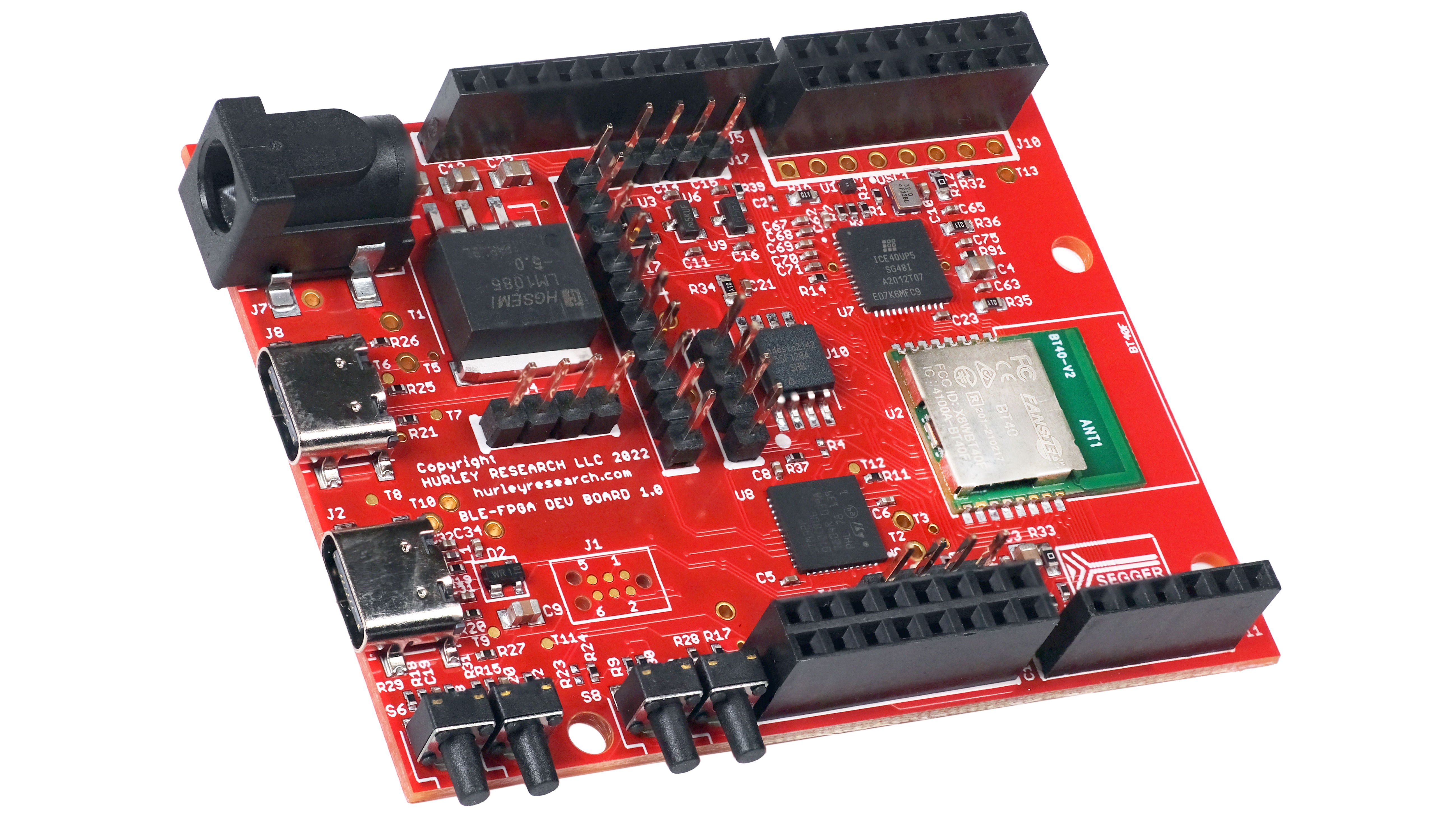
The NRFICE FPGA is a Bluetooth FPGA board designed for edge computing and IoT applications. It is built upon a combination of the dual-core nRF5340 Bluetooth SoC and the Lattice ICE40UP5K FPGA. The ICE40 UltraPlus is a low-power, high-performance FPGA for edge computing and artificial intelligence projects and the nRF5340 is a Bluetooth 5.3 SoC that supports Bluetooth Low Energy (BLE), Bluetooth Mesh, Thread, NFC, and Zigbee. Through the Nordic nRF5340, NRFICE can load a project directly into the iCE40 FPGA, bypassing the usual extensive toolchain setup. This enables a new class of FPGA development, where bitstreams can be hosted in the cloud, selected by a user on their phone, and loaded wirelessly to the board. It features a built-in J-Link OB for easy debugging and programming without the need for emulator dongles and is similar to the previously covered Segger emPower evaluation board in this regard. This board supports […]
Lattice Avant mid-range FPGA platform features up to 500K logic cells, 25 Gbps SERDES, Hard PCIe Gen4
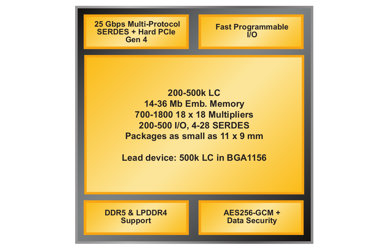
Lattice Avant is a new low-power and small form factor mid-range FPGA platform, manufactured with a 16nm FinFET process, and equipped with 25 Gb/s SERDES, hardened PCI Express, external memory PHY interfaces, a high DSP count, and a security engine. Lattice Semi is better known for its entry-level FPGAs such as the iCE40 which is popular in the community thanks to low-cost hardware and support for open-source tools, but the Avant platform marks the company’s entry into the mid-range FPGA market, defined by chips with 100k to 500k logic cells (LCs). Lattice Avant highlights: FPGA fabric – 200K to 500K logic cells up to 350 MHz DSP – 700 to 1,8000 18×18 multipliers @ up to 650 MHz to support the latest AI algorithms Memory 14-36 Mbit embedded memory up to 650 MHz DDR3L/DDR4/LPDDR4 and DDR5 support I/Os 4x to 28x 25 Gbps multi-protocol SERDES Hard PCIe Gen4 200 to […]
iCESugar-nano is a $19 iCE40LP1k FPGA board with 3x PMOD connectors
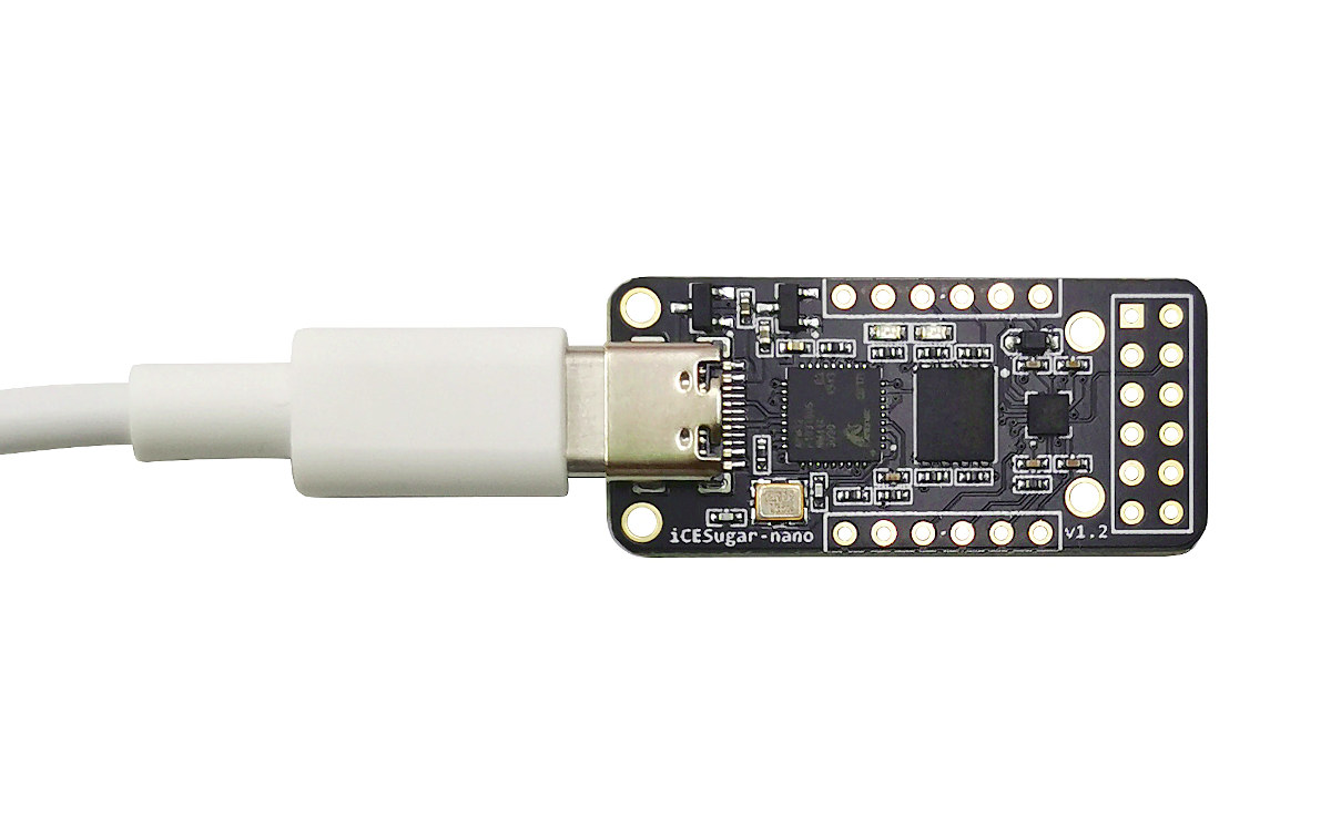
Muse Lab’s iCESugar-nano is a tiny FPGA board based on Lattice Semi iCE40LP1K-CM36 programmable via its USB-C port through on-board iCELink debugger, and exposing I/Os for three standard PMOD connectors. The board is fully supported by Yosys open-source toolchain ( Yosys+ nextpnr + IceStorm), and the onboard debugger supports drag-and-drop programming so that you can just drag the FPGA bitstream into the virtual disk to program it through a USB Type-C cable. iCESugar-nano specifications: FPGA – Lattice Semi iCE40LP1k FPGA with 1280 LUT/8KB SRAM/PLL Storage – 2MB SPI flash (W25Q16) USB – 1x USB Type-C port for power and programming Expansion – 14x usable IOs with 1x 12-pin PMOD connectors and 2x 6-pin PMOD connectors Debugging – On-board iCELink debugger based on Arm Mbed DAPLink Misc – Adjustable clock (8/12/36/72MHz), LED Power Supply – 5V via USB-C port Dimensions – 3.9 x 1.8 cm Documentation, schematic PDF, links to tools, […]
Lattice Introduces CrossLink-NX FPGA for Edge AI & Embedded Vision
Lattice CrossLink-NX FPGA Lattice Semiconductor has announced the first product associated with its Nexus Platform, the CrossLink-NX FPGA designed for embedded vision and Edge AI applications. There are two offerings at this time, the CrossLink-NX FPGA 17, and the CrossLink-NX FPGA 40. Recent Announcements The Nexus Platform was introduced at the beginning of December 2019, and now CrossLink-NX has been developed and is being manufactured. The first announcements of Lattice Nexus Platform and The CrossLink-NX Product Family came as the company’s moved to capture the embedded vision systems market. The Standout Features The low-power consumption, low soft error immunity, and 10Gbps MIPI are highlights of the CrossLink-NX FPGA. Other features include Instant On, with IO configured in 3 ms, and a total of 8 ms for the device. The Cross-Platform FPGAs The trends in technology are leading to devices that can cross function in a number of different tech environments. […]
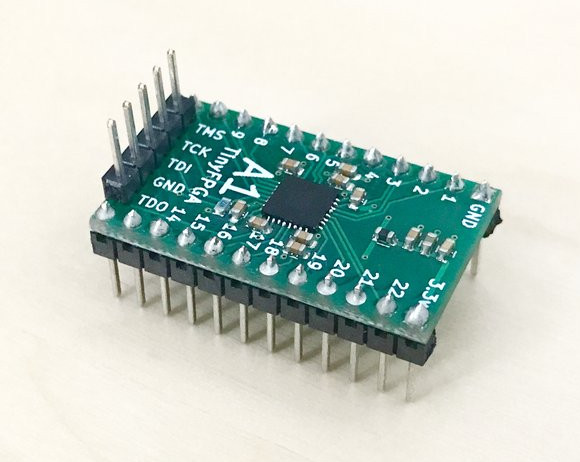
TinyFPGA is a Breakout Board for Lattice Semi MachXO2 FPGA
We’ve covered several low cost FPGA boards over the years, but if you want a platform with the bare minimum, you may be interested in tinyFPGA breakout board based on Lattice Semi MachXO2 FPGA board that comes with two flavors: A1 with MachXO2-256, and A2 with the more powerful MachXO2-1200 FPGA. TinyFPGA board specifications: FPGA A1 board – Lattice MachXO2-256 with 256 LUTs, 2 kbits distributed RAM A2 board – Lattice MachXO2-1200 with 1280 LUTs, 10 kbits distributed RAM, 64 kbits EBR SRAM, 64 kbits flash memory, and a PLL (See datasheet for MachXO2 family) Built-in flash configuration memory programmable via JTAG I/Os 18 user IOs (21 with JTAGEN) 1x SPI Hard-IP 2x I2C Hard-IPs A2 board only – 1x PLL Hard-IP Power Supply – 3.3V Dimensions – ~3.05 x 1.8 cm You’ll need a JTAG programmer for Lattice FPGA as well as Lattice Diamond software – available for Windows […]


