
Tejinder has just sent me a picture of the internal boards of the CoolShip Android keyboard computer. It’s composed of a main board (Keyboard-V2.0) and a CPU module with RK3066, flash and SDRAM chipsets, PMIC, and video decoder..
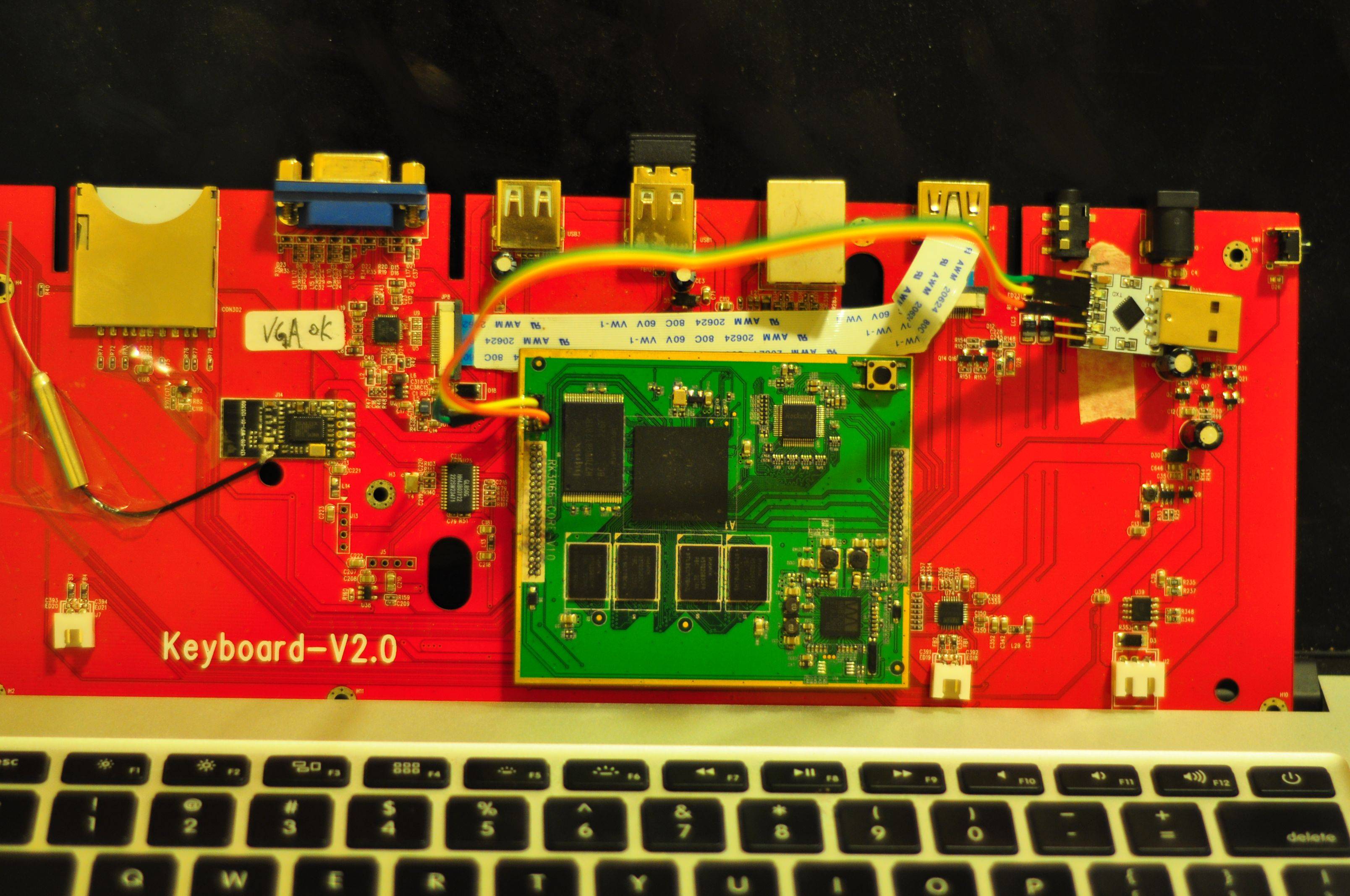
Tejinder found the following components on the boards:
- Processor – Rockchip RK 3066
- SDRAM – 4x Hynix H5TQ2G83BFR
- Flash – Hynix h27ubg8t2btr
- 1080p Video decoder – Rockchip RK1000S
- PMIC – 1x Wolfson WM8326G
- DAC – 1x Wolfson WM8960G
- Wifi chip – RTL8188CTV
- USB HUB – GL850G
The two 2-pin connector (one on the left, and the other under the DAC) should be for the speakers, and the 3-pin connector on the right goes to a 8-pin IC connected to the power, so it could be the connection to the 300 mAh battery used to handle unexpected power failure.
You’ll also notice he has connected an UART to TTL debug board to the Rockchip CPU module to access to the serial console, so goodness may come out of this 🙂

Jean-Luc started CNX Software in 2010 as a part-time endeavor, before quitting his job as a software engineering manager, and starting to write daily news, and reviews full time later in 2011.
Support CNX Software! Donate via cryptocurrencies, become a Patron on Patreon, or purchase goods on Amazon or Aliexpress. We also use affiliate links in articles to earn commissions if you make a purchase after clicking on those links.


The Coolship SOM design seems to have some advantages over existing standards (eg EDM; see comments in orignal Coolship post). I think Focuswill is quite an innovative company, wish them every success, and could understand if they didn’t want to open source this design – allowing competitors to produce similar products if this catches on.
But could the SOM setup be reverse engineered to produce an open standard? (& would it be worth it? :s )
@onebir
Focuswill SoM design may have some advantages for this particular product, but it probably doesn’t have the flexibility of other standards such as EDM or SMARC (previously ULP-COM).
They made vga out but rk3066 doesn’t have it. Its interesting how they done it?
I don’t really understand this wide ribbon cable. I admit I didn’t check their website, anyways it looks strange connecting two points on the same PCB. Did they run out of space on the layers to route it properly? Or it has some deeper meaning which I missed?
@KiLLWarez
They must have used the LVDS interface, and used an LVDS to VGA chip for the conversion. There’s a chip on the right on the “VGA OK” sticker, but I can’t read what it is on the picture.