
Intel Tremont microarchitecture was first leaked in April 2018 as a successor to Goldmont Plus used in Gemini Lake processors among others. But Intel has now made it official and revealed details about Tremont architecture at Linley Fall Processor Conference in Santa Clara, California.
The new architecture is said to deliver significant IPC (instructions per cycle) gains compared with Intel’s prior low-power x86 architectures. Tremont-based processors will target client devices, IoT products, 5G networking, efficient datacenter servers, etc…
Tremont Architecture
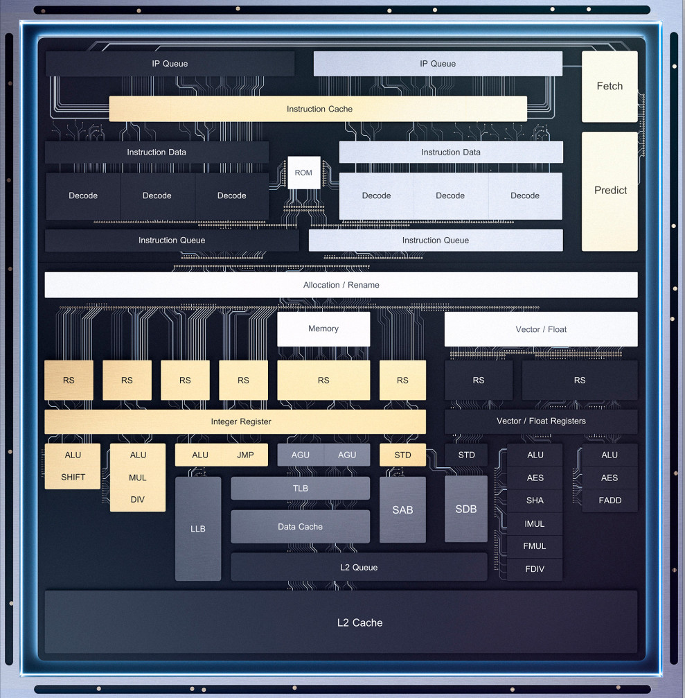
Some of the highlights of Tremont architecture include:
- Intel Core class branch prediction with long history,32 bytes based, L1 predictor (no penalty) and large L2 predictor
- Out of order fetch – 32KB instruction cache, 32 bytes/cycle, up to 8 outstanding misses
- 6-wide out of order instruction decode
- Dual 3-wide clusters
- Wide decode without the area of a uop cache
- Optional single cluster mode based on product targets
- 4 wide allocation
- 10 execution ports
- Dual load/store pipelines
- 32KB data cache
- 1024 entry second level TLB
- Quad-core module
- L2 cache between 1.5 MB and 4.5MB
- Crypto acceleration – Dual 128bit AES units, 4 cycle; Single instruction SHA256, 4 cycle Galois Field new instructions
- Parallel reservation stations & execution ports
- 3 SIMD/AES/FMUL
- SIMD/AES/FADD
- Store data
New instructions and technologies include:
- Accelerator interfacing Instructions – Efficient and scalable work-dispatch and synchronization to accelerators
- Intel Speed Shift improves responsiveness with faster hardware controlled frequency changes
- CPU rooted secure boot via Intel Trusted Execution Technology and Intel Boot Guard
- Intel Total Memory Encryption improves confidentiality protection in memory from physical attacks
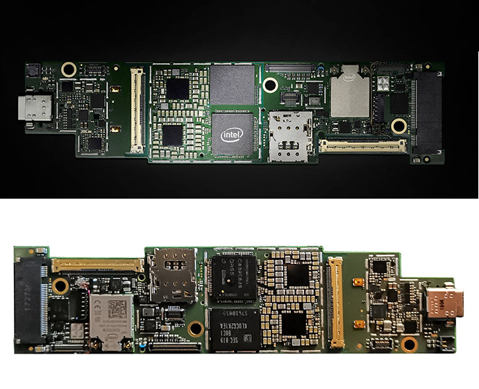
Lakefield Hybrid Processor
Lakefield processors will be the first to be built around Tremont architecture and manufactured with a 10 nm process as well as Intel Foveros 3D packaging technology combining little and big cores. The first Lakefield processor will have one Sunny Cove core and four low power Tremont cores combined with a 64-EU Intel Gen11 graphics, Gen11.5 display core supporting 5k60 and 4k120 video output, and a media core capable of handling 4K60 and 8K30 video decoding.
The most impressive improvement is the standby power as Lakefield will consume 1/10th in standby compared to Gemini Lake. Graphics performance will improve by 50%, and the core area will be reduced by 40%. The company also mentions a 40% Z reduction, but I don’t really understand what that means in that context unless they talk about the height of the package.
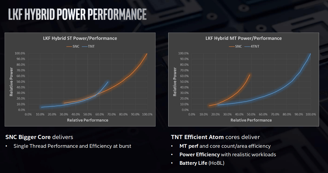
The chart above shows the performance and power consumption of the Sunny Cove core (SNC) and Atom cores (TNT) in the Lakefield processor both in single-thread mode, and with the SNC core compared to four TNT cores. This show the SNC will likely be activated for demanding single-thread tasks due to its higher performance, while the TNT cores will handle low power tasks, and tasks that benefit from multiple cores since those four cores can deliver better performance at much lower power consumption.
More details may be found in the announcements for the new architecture and processor.

Jean-Luc started CNX Software in 2010 as a part-time endeavor, before quitting his job as a software engineering manager, and starting to write daily news, and reviews full time later in 2011.
Support CNX Software! Donate via cryptocurrencies, become a Patron on Patreon, or purchase goods on Amazon or Aliexpress. We also use affiliate links in articles to earn commissions if you make a purchase after clicking on those links.


The description of the Tremont makes it look much more like a low-power Core than an atom. It has wide exec units and out-of-order. This is a nice move!
As a stand-alone atom — yes. As a little core — absence of avx will hurt it.
Looks interesting. Getting down to the same power envelop as ARM while still being about to run those nasty x86 instructions might hurt “ARM in the datacenter” etc etc. The density of the passives around the components on those boards impressed me the most. :p
I thought the same when seeing the capacitors. I’m wondering to what extent they participate to the thermal dissipation 🙂
>I’m wondering to what extent they participate to the thermal dissipation ?
It would be nice to see the thermal simulations, current return path simulation etc for something like this.
I’m in the 4 layers winging it gang so seeing how the 12+ layers doing it for real gang live would be an experience.
Hopefully Intel will actually ship these on volume. Apollo lake and Gemini lake chips have been in somewhat short supply.