A couple of weeks after unveiling Arduino UNO WiFi with ESP8266 and Atmel AVR, Arduino Srl has introduced Arduino PRIMO board with Nordic Semi nRF52 MCU with Bluetooth Smart and NFC, ESP8266 for WiFi, and STM32 to handle GPIOs and USB UART during May Faire Bay Area 2016.
Arduino Primo board (A000135) specifications:
- Service Micro-controller
- STMicro STM32F103R8T6 ARM Cortex-M3 MCU @ 72 MHz with 64KB flash, 20KB SRAM
- USB/Uart converter & CMSIS-DAP
- GPIO expander, IrDA
- Board power management
- Operating Voltage – 2.0 to 3.6 V
- Arduino Micro-controller
- Nordic nRF52832 ARM Cortex-M4F MCU @ 64 MHz with 512 KB flash, 64KB SRAM
- Analog I/O Pins – 6 + 1 DAC
- DC Current per I/O Pins – 7 mA
- Bluetooth Smart – Up to +4 dBm output power, -96 dBm sensitivity
- Other features – PDM interface, AES HW enc, NFC tag
- WiFi Micro-controller
- Espressif ESP8266 Tensilica Xtensa LX106 WiSoC @ 80 MHz with 8MB RAM for instructions, 12MB for data
- Storage – 4MB SPI flash
- WiFi 802.11 b/g/n 2.4 GHz
- Wake up time – < 2 ms
- Operating Voltage – 3.3 V
- Common Specs
- Digital I/O – 20 pins
- PWM Output – 3
- Misc – On-board button, LED
- Input Voltage – 5V
- Power Consumption – 87 mA @ 5V typ.
- Dimensions – 68.5 x 53 mm
- Weight – 34 grams
The board is not yet available, and documentation is limited to what’s on the product page. But we can safely assume that the board will be programmable via the Arduino IDE, and Nordic also mentioned that professional developers and Makers will also be able to use any Nordic nRF52 Series-compatible Software Development Kit (SDK) or programming tools, for example to develop IPv6 over Bluetooth low energy applications.
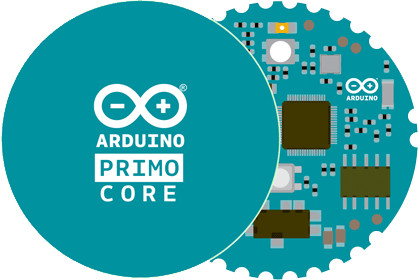
Arduino Srl and Nordic Semi are also working on a coin-cell powered Arduino Primo Core module with nRF58232 chip and motion and environmental sensors.
Considering the recent legal history between Arduino Srl and Arduino LLC, I’m a little surprised they went with Arduino Primo, as Arduino LLC is also selling a toy designed to teach programming logic to young children, also called Primo.
AFAIK, no information about the launch date and pricing have been released so far.

Jean-Luc started CNX Software in 2010 as a part-time endeavor, before quitting his job as a software engineering manager, and starting to write daily news, and reviews full time later in 2011.
Support CNX Software! Donate via cryptocurrencies, become a Patron on Patreon, or purchase goods on Amazon or Aliexpress. We also use affiliate links in articles to earn commissions if you make a purchase after clicking on those links.



Do you know how many ADC channels and what resolution ?
See you have given the BT Tx power and Rx sensitivity; do you have the same for the WiFi ?
I read the ESP8266 can be quite greedy on current consumption, needing a psu supplying over 1/2 Amp, so how does this board manage a thrifty 87 mA ?
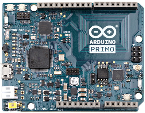
I can see just 1 Antenna socket, is this for the Wifi, BT, or both ?
ESP32 will rule them all.
1 antenna for bluetooth top left
1 antenna for WIFI bottom right
Up to +4 dBm output power, -96 dBm sensitivity for bluetooth
ADC 6 + 1 DAC
Digital I/O Pins: 20
PWM pin : 3
Power Consumption :87 mA
Well, that’s certainly a kitchen sink approach, isn’t it? A separate 32-bit MCU for each interface, USB, WiFi, and BTLE. Does it also appear to have a battery charger IC? And is that a full bridge rectifier made up of those 8 beefy diodes, can it run off AC? They missed an opportunity to include a fourth MCU to interface between 5V headers and the 3V3 MCUs 🙂
I’m unimpressed with this division of duties between so many MCUs, it seems unnecessary in this case, but I guess that’s always been Dog Hunter (or I guess they’re now named Arduino Srl)’s preferred approach, starting with the Yun. I understand the “political” need to run the Arduino code on the NRF52 if Nordic Semi were the sponsor of this design, but it seems just silly to have all these separate MCUs and then still end up having one of the MCUs have to split computational time between threads for running the radio (softdevice in Nordic parlance) and the user’s code. How many Not/Connected I/O pins do you suppose this design is wasting? And I have to wonder how many black boxes will be on the schematic of this board, that does seem to be a mainstay of Dog Hunter’s approach to “open-source” hardware.
@paul: the trace from the u.FL (and the chip antenna below it) looks like it goes directly to the ESP8266 chip, so I’d guess it’s for wifi only. Also there’s the silk-screen label reading “WIFI” next to it. The other MCU up in the top-left must be the nRF52. I was totally unaware the nrf52 supported NFC, that’s cool, though I’m not up enough on NFC specs to understand how comprehensive its support is. The NRF52 looks to have a chip antenna (just below the RST button/beside the 0.05″ debug header) on the BLE/2.4GHz pin and then that monster PCB loop antenna for the NFC/13.56MHz on the right side of the chip.
Sounds like the only ADC with accessible pins broken out is via the nrf52 (but all 3 chips do have ADCs built-in). 8/10/12-bit resolution, with 14-bit oversampling available. The specs for the board above say “6 Analog pins”, so I’m not sure the total number of channels matter if they aren’t all accessible anyway, but the datasheet says the nrf52 supports 8 channels. Its datasheet is at http://infocenter.nordicsemi.com/pdf/nRF52832_PS_v1.0.pdf .
No guess on the power, but the board could suck down 500mA while transmitting and still be advertised as 87mA “typical”. That power circuitry is weirdly elaborate and beefy. And there do appear to be a lot of FETs spread around the board, so maybe the STM32 is toggling bits and pieces on and off as part of its “board power management”. Or maybe there’s just a ton of different voltages to support for each of the different MCUs and radios.
I could not find the block diagram yesterday, but here it is @
@John S.
Thanks for your observations. I see from the since attached block diagram there are 2 32KHz crystals, so what with the hint of integrated battery backup, maybe a RTC is supported ? I seem to remember when reading specs of early standalone ESP8266 that the module had very good Rx Sensitivity – but with a big disadvantage of requiring a very beefy PSU to supply its peak current requirement; but can one assume newer ESP8266’s integrated into a Arduino have the same spec/characteristics as the older standalone versions ? The ESP8266 ADC was single-channel, and low-res.
This boards appears very interesting in appearing to have almost everything I need, but is presently too short on specs.
@John S.
Since previous reply above, seen the hackerboards article on it, which links to both a zoomable version of above block diagram which appears to confirm the SBC can autoswitch between external and battery power, and to detailed specs for the STML0 & nRF52 SoCs confirming both support RTC and indicating very good low-power modes; but unfortunately no link to detailed spec for the integral ESP8266 chip – the one I read can consume very high peak currents.
If I remember rightly I read on various furums that USB WiFi dongles generally consume 40mA – so WHY does the ESP8266 require a supply capable of 500mA ?