
 Ambiq Micro is using sub-threshold voltages under 0.5V to offer ultra-low-power Arm microcontrollers. In 2015, the company launch the Apollo Cortex-M4F MCU with 30µA/MHz power consumption in active mode, which was followed in 2016 by Apollo 2 in consuming just 10µA/MHz, and Apollo 3 (Blue) dropped power consumption to as low as 6µA/MHz against using a Cortex-M4F @ 48 MHz in active mode.
The fourth generation of ultra-low-power Apollo microcontroller has now been announced with Apollo 4 and Apollo 4 Blue microcontrollers – the latter adding Bluetooth – halving the power consumption of Apollo 3 at just 3µA/MHz, or ten times less than the original ultra-low-power MCU from the company.
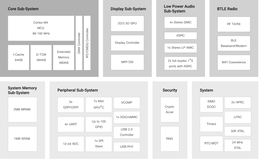
Apollo 4 (Blue) specifications and key features:
- MCU Core – Arm Cortex-M4F core up to 192 MHz (TurboSPOT) with FPU, Memory Protection Unit (MPU), and Secure Boot
- GPU – 2D/2.5D graphics accelerator with full alpha blending, texture and frame buffer compression
- Ultra-Low Power Memory
- Up to 2MB of non-volatile MRAM for code/data
- Up to 1.8MB of low power RAM for code/data
- Display I/F – 2-lane MIPI DSI 1.2 up to 500 Mbps, up to 640 x 480 resolution with 4-layers with alpha blending, frame buffer decompression
- Audio
- 1x stereo low power Analog microphone
- 4x stereo Digital microphones
- 2x full-duplex I2S ports with ASRC
- Wireless Connectivity (Apollo 4 Blue only)
- Bluetooth Low Energy 5 up to 2 Mbps, extended advertising packets, AOA/AOD for direction finding
- Tx – 4 mA @ 0 dBm, Rx 4 mA
- Tx – -20 dBm to +10 dBm output power
- Rx Sensitivity – -97 dBm at 1 Mbps, -94 dBm at 2 Mbps
- Ultra-Low Power Interface for On- and Off-Chip Sensors
- 12-bit ADC, 11 selectable input channels
- Up to 2.8 MS/s sampling rate
- Temperature sensor with +/-3°C accuracy
- Ultra-Low Power Flexible Serial Peripherals
- 3x 2/4/8-bit SPI master interfaces
- Up to 8x I2C/SPI masters for peripheral communication
- 1x SPI slave for host communications
- 4x UART modules with flow control
- 1x USB 2.0 HS/FS device controller
- 1x SDIO (SD3.0)/1x eMMC (v4.51)
- Clock Sources – 16-52 MHz and 32.768 kHz Crystal (XTAL) oscillators; 1 kHz LFRC oscillator; 2x HFRC oscillator – 192/384 MHz
- Ultra-Low Supply Current
- 3 μA/MHz executing from MRAM (with cache)
- 3 μA/MHz executing from SRAM
- 1.5 μA low power sleep mode with RTC and 8KB SRAM retention
- Operating Voltage – 1.71-2.2 V; SIMO buck; Multiple I/O voltages supported
- Package Options
- Apollo 4
- 5 x 5 mm, 146-pin BGA with 105 GPIO
- 3.9 x 3.9 mm, 121-pin WLCSP with 82 GPIO
- Apollo 4 Blue – 4.7 mm x 4.7 mm, 131-pin SIP BGA
- Apollo 4
- Temperature Range –40°C to 85°C
- Process – TSMC 22nm ULL
Apollo 4 and Apollo 4 Blue are basically identical except for the latter adding Bluetooth 5 LE, and losing one I2C interface in the process. Packages are also different.
Applications listed by the company include smartwatches, wireless sensors and IoT, activity/monitors, motion and tracking devices, alarms and security systems, far-field voice remotes, consumer medical devices, predictive maintenance, and the smart home. The press release highlights Apollo 4 is especially well-suited to battery-powered smart IoT devices with always-on voice processing.
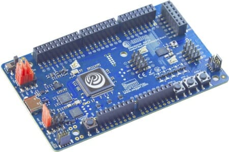
The company offers a development board for the new Apollo 4 microcontrollers with I/O headers, buttons, and USB-C port. There’s no public documentation for the board that I could find, however.
Visit the product page for further information.

Jean-Luc started CNX Software in 2010 as a part-time endeavor, before quitting his job as a software engineering manager, and starting to write daily news, and reviews full time later in 2011.
Support CNX Software! Donate via cryptocurrencies, become a Patron on Patreon, or purchase goods on Amazon or Aliexpress. We also use affiliate links in articles to earn commissions if you make a purchase after clicking on those links.


The title advertises the chip as particularly fit for battery-powered devices. Of course the low power CPU can help, but the much more critical sleep current is not that low compared to similar devices. What is really exciting is the onboard MRAM. It makes the chip a great platform for batteryless devices. Currently, most development in that domain is done on the dated MSP430 with FRAM.
Cool, have to check this out!
Unfortunately they didn’t sell the last ones via normal distributors (mouser, digikey, etc), rather only through salespeople that you had to call up and ask for quotes and such. So I suspect this is similarly DOA for people not buying millions of units.
It also looks to be in the ‘if you have to ask how much it costs, you can’t afford it’ category.
I may be wrong, but I think a 22nm process for microcontrollers is quite unusual, and likely contributes to the cost.
Oh, no doubt it does. I’d think that most of them are done in 90mn or larger. IIRC, Microchip used to put out a report on the fabs they owned and what their capabilities and utilizations were. They had aquired so many fabs over the years as they aquired small little chip makers. Each fab could pretty much only make that companies chips, so it was a real issue for their customers to understand what their capabilities were (don’t come asking for 1M of this opamp as we only have this tiny little factory that can only make 10K/month).
They had fabs up to around a half micron! I.E. 500nm. Most of their capacity was between 250 and 120nm, though.
I wonder if anyone who subscribes to one of the chip RE newsletters knows what something like an STM32F103 type of chip is fabbed on.
Hey, how about that, the wikipedia page for STM32 has some fab info! https://en.wikipedia.org/wiki/STM32
But there isn’t any for the F103. The family above it–F2 at up to 120MHz uses 90mn–and the family below it–F0 at 48MHz uses 180nm. Most everything is 90mn. Only the H7 family is at 40nm (400MHz).
I’m curious who’s 22nm process that is. Is it Intel? (didn’t think they were doing that much charter work). GF would make sense as they have SoI which is generally good for lower leakage applications. But that’s not at sub-threshold logic–which is a very hard topic to find good info on. Up until recently, the biggest users of sub-threshold logic were implanatable medical device manufacturers and they are a very closed lipped community!
That’s TSMC process.
But I would still pay more on a normal distribution platform. I mean for this energy consumption: Of course. I guess 22nm etc. need to get more mainstream and cheaply accessible. Maybe it will happen once they get 7nm more accessible.
Definitely
They must deliver to boeing and the dod…
Lol how I hated this type of phone only companies.
Speaking of weird distribution channels, Sparkfun manufacture and sell an Ambiq Apollo 3 Blue 10x15mm module (Sparkfun’s “Artemis” line). They sell the modules for ~$9, which must mean the chips are pretty cheap considering how much Sparkfun markup every other simple breakout board they manufacture or sell, and this one’s even FCC-certified.
It was initially (and only very briefly), Google’s flagship chip for Tensorflow “Lite”, but I’m not clear if Google led Sparkfun to the chip or if Sparkfun led Google to it.
The two companies released an official demo board together with the chip prior to Sparkfun releasing their module, but it could have been in development at Sparkfun and the board just had to release in time for a Tensorflow conference before the module was finished.
How much is power consumption from others Cortex-M4F used in the market? I looked it up and only finded some old MCUs as example
I’m confused about the claimed sub-threshold voltage of less than 0.5V given that the chip is supposed to operate between 1.7 and 2.2V. OK 1.7V is low but it’s far from being sub-threshold and we currently find regular processors running between 0.9 and 1.1V, thus even lower. Or maybe the MCU can be powered as low as 0.5V at very low frequency and the claimed power draw only concerns this range ? I would expect that the chip can run at 192 MHz at less than 600uA under 1.7V but with the contradicting info above I’m now having serious doubts :-/
I understand 0.5V (edit: it looks like they dropped it to 0.3V now) is used internally to switch on/off transistors, but supply voltage for the chip is higher.
The MCU has internal voltage converters that step down the voltage. Diferrent parts of the MCU requires different supply voltages. Typically anything that interfaces with the outside world runs close to the supply voltage, whereas a CPU typically runs at 0.9V-1.1V, and a radio runs at f.ex. 1.3V.
Running a CPU core at 0.3V and still have it run deterministically is a huge achievement. I honestly assume that there’s tons of bugs in this device though. You should take this sales brief as what it is though, marketing.
Yeah I agree that running *any* logic chip on sub-threshold is a huge achievement. Square signals look like noisy amortized sine waves, and keeping all outputs in sync on any bus must be quite difficult. And doing this at 200 MHz is even more impressive if that’s true.
Well, the 200 MHz would explain the need for the 22nm process when normal logic can do that at 90nm easily.
As an example, Intel was doing >200MHz on .350uM.
The development board looks identical to the Apollo 3+ development board (which is documented on the Ambiq site). There’s nothing special about it, except that it has Segger J-Link on board.
It now jumped back up to 5uA/MHz, I wonder what happened and when it will be available…