
Intel has a mixed history with its ability to keep production schedules for new processes, with notably its 10nm process suffering from years of delays before finally being deployed into chips.
But the US company has now held an event unveiling the process & package roadmap through 2025 and beyond, which includes 7nm, 4nm, 3nm, and even the switch the angstrom scale (1A = 0.1 nm) with a 20A process expected in 2024/2025.
Intel Process roadmap to 2025 and beyond
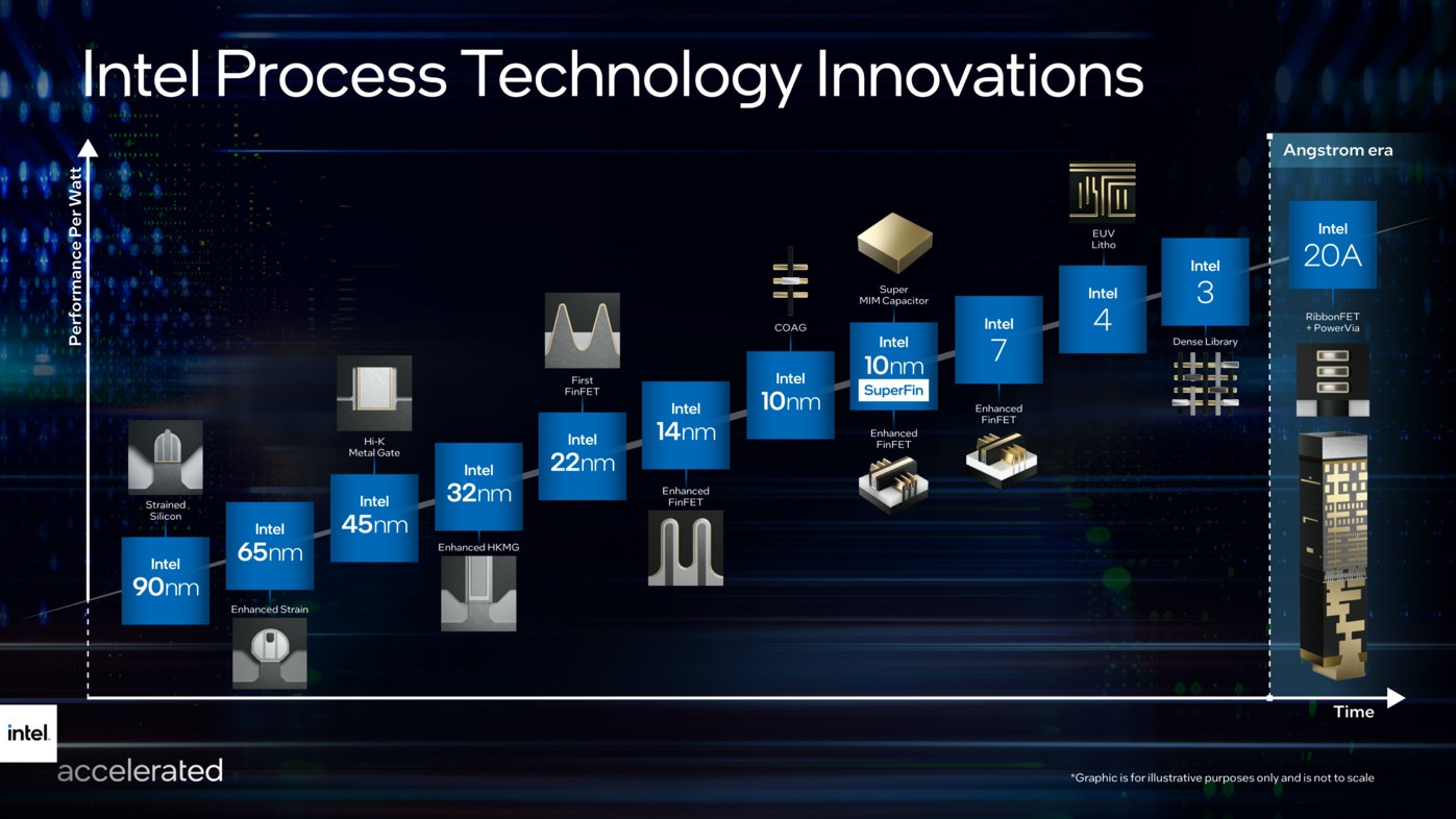
On the process node sides of things, here’s what to expect in the next few years:
- Intel 7 delivers 10% to 15% performance-per-watt improvements, and will be found in Alder Lake for client in 2021 and Sapphire Rapids for the data center, with the latter expected to be in production in Q1 2022.
- Intel 4 promises a 20% performance-per-watt increase over Intel 7, and is the first Intel FinFET node to use extreme ultraviolet lithography (EUV), which involves a “highly complex optical system of lenses and mirrors that focuses a 13.5nm wavelength of light to print incredibly small features on silicon”. Intel 4 will be ready for production in H2 2022 for products shipping in 2023, including Meteor Lake for client and Granite Rapids for the data center.
- Intel 3 is expected to deliver an 18% performance-per-watt boost compared to Intel 4, and will be ready to begin manufacturing products in H2 2023. Intel has yet to announce which processor families will benefit from the new process node.
- Intel 20A is expected in 2024 with RibbonFET and PowerVia technologies. RibbonFET is a gate-all-around transistor delivering faster transistor switching
speeds while achieving the same drive current as multiple fins in a smaller footprint compared to FinFET. PowerVia is an implementation of backside power delivery, eliminating the need for power routing on the front side of the wafer and providing optimized signal routing while reducing droop and lowering noise. - Intel 18A is already in development with refinements to RibbonFET that will deliver another “major jump” in transistor performance in 2025.

Note that the marketing team seems to have been involved here, as Intel 7 used to be called “10nm Enhanced SuperFin”, while Intel 4 was previously named “Intel 7nm” process node. I suppose it depends on how you measure it, and in the past, Intel explained competitors had a different way of measuring the transistor size.
Intel package innovations
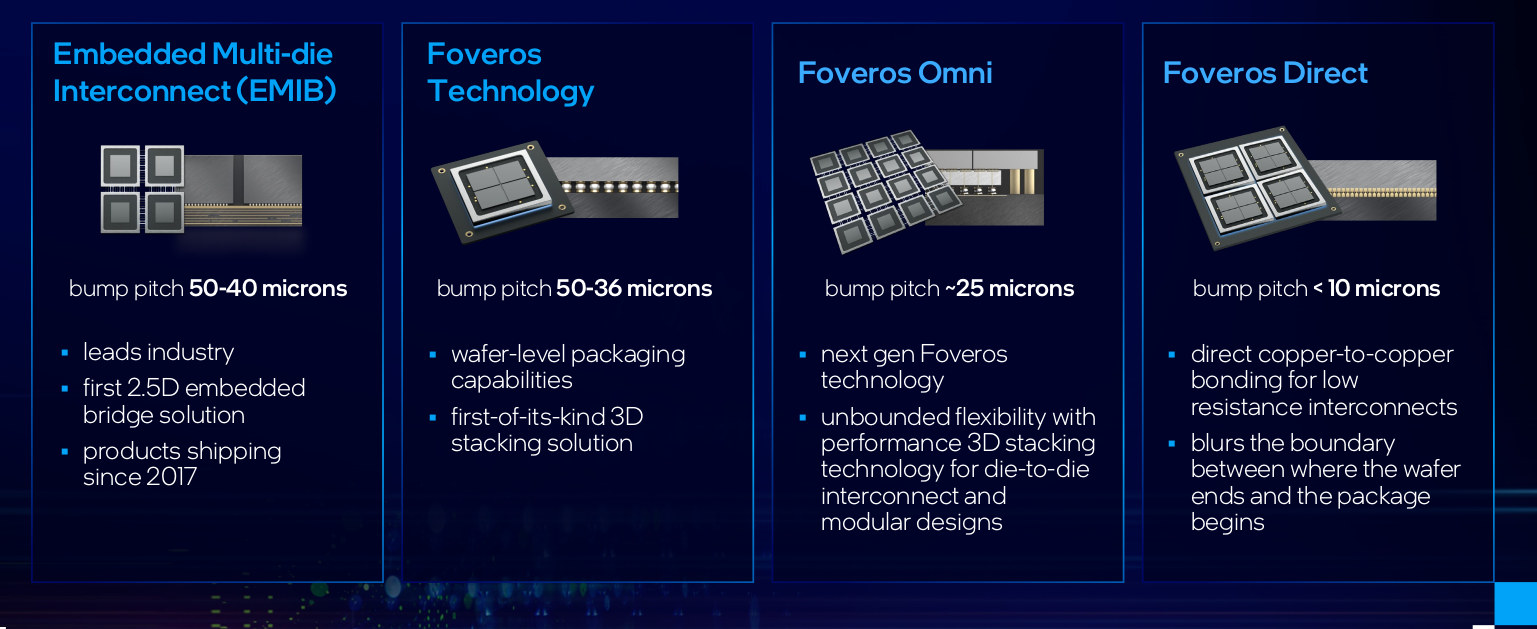
Intel also talked about package innovation like the existing Foveros 3D stacking technology found in the about-to-go-EOL Lakefield processors:
- EMIB (embedded multi-die interconnect bridge) found in Intel Xeon Sapphire Rapids for the data center. The next generation of EMIB will move from a 55 micron bump pitch to 45 microns.
- Foveros is not exactly as we’ve just noted, but the second generation of the 3D stacking technology will be found in Meteor Lake client products and features a bump pitch of 36 microns, tiles spanning multiple technology nodes, and a thermal design power range from 5W to 125W.
- Foveros Omni builds upon Foveros technology to allow die disaggregation, mixing multiple top die tiles with multiple base tiles across mixed fab nodes. Volume manufacturing of processors based on Foveros Omni should start in 2023.
- Foveros Direct will be complimentary to Foveros Omni and be ready at about the same time. It relies on direct copper-to-copper bonding for low-resistance interconnects, and enables sub-10-micron bump pitches, providing an order of magnitude increase in the interconnect density for 3D stacking.
More details can be found on Intel website, as well as Anandtech which looks at how the new Intel processes compared to TSMC, Samsung, or even IBM processes, and more.

Jean-Luc started CNX Software in 2010 as a part-time endeavor, before quitting his job as a software engineering manager, and starting to write daily news, and reviews full time later in 2011.
Support CNX Software! Donate via cryptocurrencies, become a Patron on Patreon, or purchase goods on Amazon or Aliexpress. We also use affiliate links in articles to earn commissions if you make a purchase after clicking on those links.


Wishful thinking. Intel trying to make its marketing even more confusing, to hide their lack in technology. But it’s so obvious people aren’t falling for it 🙂
I can see the USA government intervene to save Intel sooner than later.
People already say that Intel 10nm is the rough equivalent of TSMC 7nm. So Intel renamed it to Intel 7. And so on.
As for the rest, they have to get it out the door instead of delayed for years. I don’t know if angstroms will catch on but those are just 2nm and 1.8nm. They were planning to call one of the nodes 1.4nm before, probably to emphasize it being 100 times more dense than 14nm or something like that.
So, we see here great outcome of new tech-oriented Intel director!
He just rename processes and announce even more marketing-driven names instead of real engineering – all done.
Never mind the width just ignore the thickness building up on top.
Does that have something to do with process nodes or was it dating advice?