
A few years ago we covered Hisilicon D02 server board powered by the company’s Hip05 SoC with 16 or 32 Arm Cortex A57 cores. I had not seen any updates since then myself, but HiSilicon has released new “TaiShan” Arm based server SoCs every year, and recently unveiled Hi1620, the world’s first 7nm datacenter Arm processor, featuring 24 to 64 Arm “Ares” cores clocked at up to 3.0 GHz. Ares cores are supposed to greatly improve single thread performance in order to compete with x86 server chips.
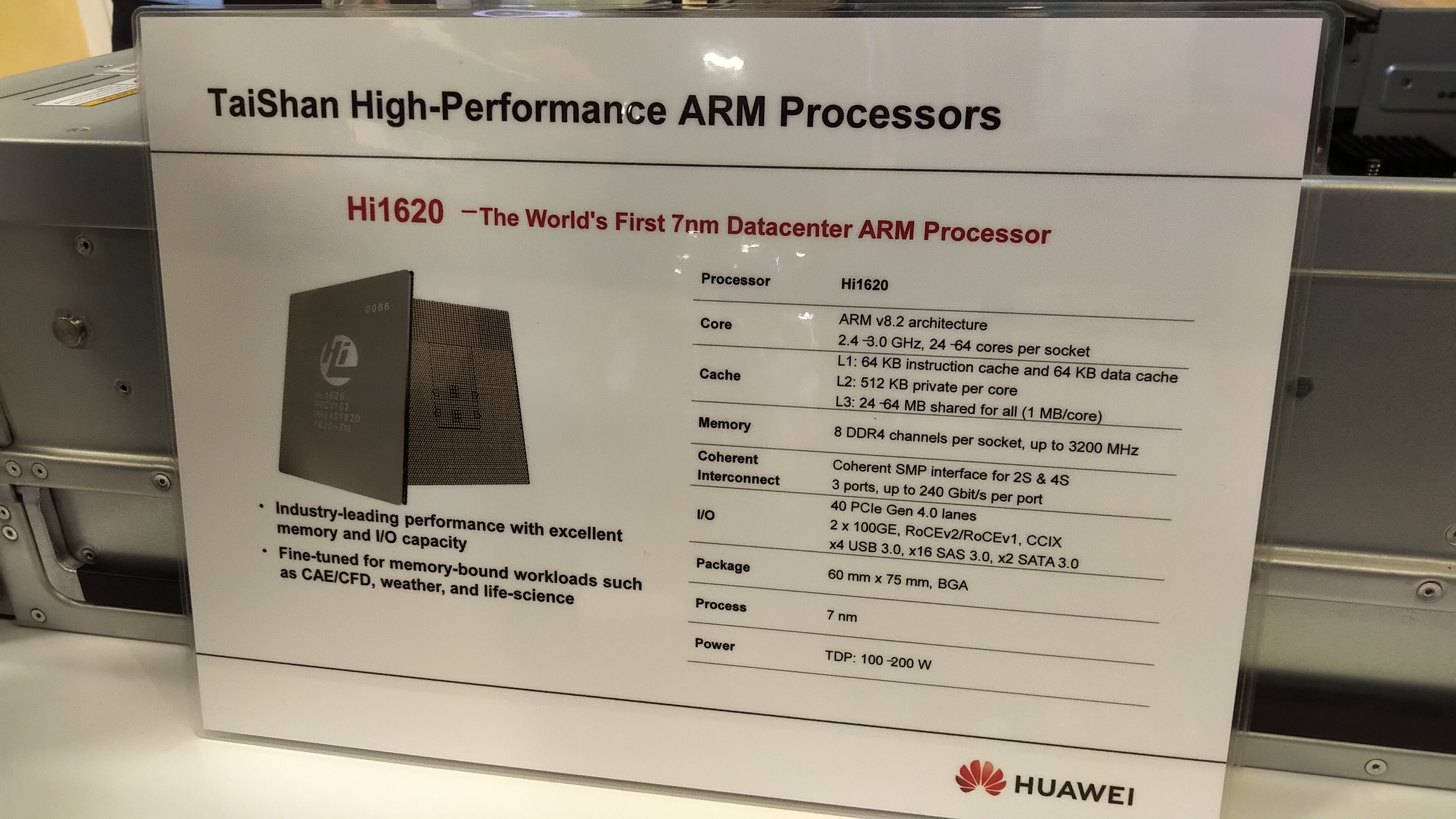
HiSilicon Hi1620 processors specifications:
- CPU – 24 to 64 Ares ARMv8.2 cores clocked at 2.4 – 3.0 GHz
- Cache – L1: 64KB I-cache, 64KB D-cache; L2: 512KB private per core, L3: 24-64 shared among cores (1MB/core)
- Memory – 8x DDR4 channels up to 3200 MHz
- Interconnect – Coherent SMP interface for 2S & 4S, 3 ports up to 240 Gbit/s per port
- I/Os
- 40x PCIe Gen 4.0 lanes
- 2x 100 GbE, RoCEv2/RoCEv1, CCIX
- 4x USB 3.0
- 16x SAS 3.0, 2x SATA 3.0
- Package – 75 x 60 mm, BGA
- Power – 100 to 200 Watts TDP
- Process – 7 nm
Anandtech reports vendors are expected Ares cores to achieve Intel Skylake levels of performance, and Hi1620 is said to be fine-tuned for memory-bound workloads such as CAE/CFD, weather and life-science.. Although an internal Hisilicon D06 development board exists, Huawei did not show any samples at the event either. So it will take some more time before it becomes available, and Arm has not provided details about Ares architecture yet. We should expect more details next year.
As a side note, Arm has made progress in high-performance computing, as there’s now one Arm supercomputer that made it to the top 500 list: Astra, built by HPE, deployed at Sandia National Laboratories, and equipped with 125,328 Cavium ThunderX2 cores delivering an HPL Linpack score of 1.5 petaflops. It’s currently listed at number 204.

Jean-Luc started CNX Software in 2010 as a part-time endeavor, before quitting his job as a software engineering manager, and starting to write daily news, and reviews full time later in 2011.
Support CNX Software! Donate via cryptocurrencies, become a Patron on Patreon, or purchase goods on Amazon or Aliexpress. We also use affiliate links in articles to earn commissions if you make a purchase after clicking on those links.


Any idea where one could find Hi1616 — the current CA72-based 32-core, 85W server chip — in the wild?
It’s used in Hisilicon D05 development board that’s probably not for sale.
For commercial products, a Baidu search reveals some Huawei “TaiShan” servers: http://zycg.gov.cn/td_xxlcpxygh/products_by_brand?category_id=7617&brand=all&page=1
I looks at TaiShan 2280 in a bit more details, and it’s officially supported by SuSE with some info in English @ https://www.suse.com/nbswebapp/yesBulletin.jsp?bulletinNumber=146997
Thanks! TaiShan 2280 does seem to be the commercial product, providing 2x Hi1616 @ 2.4GHz @ 28nm.
Anandtech lists Hi1616 and predecessors as ‘TSMC 16nm’.
Right, my bad, it’s 16nm.
16nm is what’s written somewhere 🙂
I have to admit that I have no idea how to interpret these ‘numbers’ (other than being something used by TSMC’s marketing).
According to https://en.wikichip.org/wiki/16_nm_lithography_process
‘The term “16 nm” is simply a commercial name for a generation of a certain size and its technology, as opposed to gate length or half pitch’ and ‘An enhanced version of TSMC’s 16nm process was introduced in late 2016 called “12nm”‘ and ‘TSMC uses the same BEOL as its 20nm process’.
Confusing when 20 is almost the same as 16 and then again as 12.
as far as i understand, 16/14/12 are part of finfet family and 20nm isn’t
but things gets even more complicated when you take into account density
if my memory serves me right, Intel 14nm is much more dense than TSMC 12nm (to be double-checked)
> gets even more complicated
After reading through https://www.semiwiki.com/forum/content/6713-14nm-16nm-10nm-7nm-what-we-know-now.html it seems to me this is way more complicated 🙂
Those numbers make the most sense when compared against other fabnodes by the same fab — then the ratios/savings are clear (as they’re usually quoted by the fab).
> Those numbers make the most sense
Or maybe even the only sense? After reading the above and realizing the below ’12nm process’ link being just a redirect I think those numbers make only sense when the fab is also mentioned? https://en.wikichip.org/w/index.php?title=12_nm_lithography_process&redirect=no
Intel talked about how 10nm process are not all made equal: https://www.cnx-software.com/2017/03/30/intel-my-10nm-process-is-denser-than-yours/ , and discussed that “logic transistor density” should be used instead of XX nm. But obviously this has not caught on.
That’s one area where Intel seem to show the most, erm, ingenuity, even more so than in their TDP metrics. ‘We have the best litho process if we count SRAM and flipflop transistors separately’ — Really? If an uarch requires this much SRAM to function adequately are you going to pretend your chip can work SRAM-free?
The thing that matters transistor-density-wise is entirely in the context of Performance/Power/Area (PPA):
power/transistor, performance/transistor & transistor/area -> performance/area & power/area
There’s nothing deeper that matters — at the end of the day you have N mm^2 of silicon, doing M units of work per P joules, period. That also implies that if you have the ultimate litho tech in the universe, but your uarch plain sucks, your gate size is the least of your problems.
And Intel has tried to name 10nm work for how many years now? They have so far only delivered one commercial CPU using it and it’s a turd in more ways than one. Unfortunately, for Intel that is, TSMC has overtaken them and so has Samsung by now. This stuff is really, really hard to make, even for a massive company like Intel.
That was an apparently legal move by Intel to come clean in front of their 10nm fab clients (who suffered massively due to the delays). Under no intents or purposes have Intel shipped viable 10nm products.
After Qualcomm Centriq died, maybe Huawei is the only ARM server player can compete with x86/Intel.
The interesting thing is CCIX. With CCIX integrated this processor can connect FPGA or ASIC accelerators with low latency and high throughput for heterogeneous computing. Xilinx is also adding CCIX into its FPGA and SoC.
> After Qualcomm Centriq died
https://www.anandtech.com/show/13597/just-when-you-thought-it-was-dead-qualcomm-centriq-arm-server-systems-spotted
Your post prompted me to read up on CCIX. It does appear like an unified answer to IBM’s CAPI (who used to be a founding member of CCIX consortium, but left?) and nvidia’s NVlink.
BTW, any particular reason to disregard Cavium/Marvell and Ampere as competent server-chip vendors? : )
this is sooo nice, but when VMWare will release the ARM ESXi? I’m waiting it so impatiently for my lab 🙁