
There have been attempts to bring Arm processors to desktop PC’s in recent years with projects such as 96Boards Synquacer based on SocioNext SC2A11 24-core Cortex-A53 server processor or Clearfog-ITX workstation equipped with the more powerful NXP LX2160A 16-core Arm Cortex A72 networkingprocessor @ 2.2 GHz.
Those solutions were also based server and networking SoCs, but there may soon be another option specifically designed for Arm Desktop PCs as a photo of an Arm Micro-ATX motherboard just showed up on Twitter.
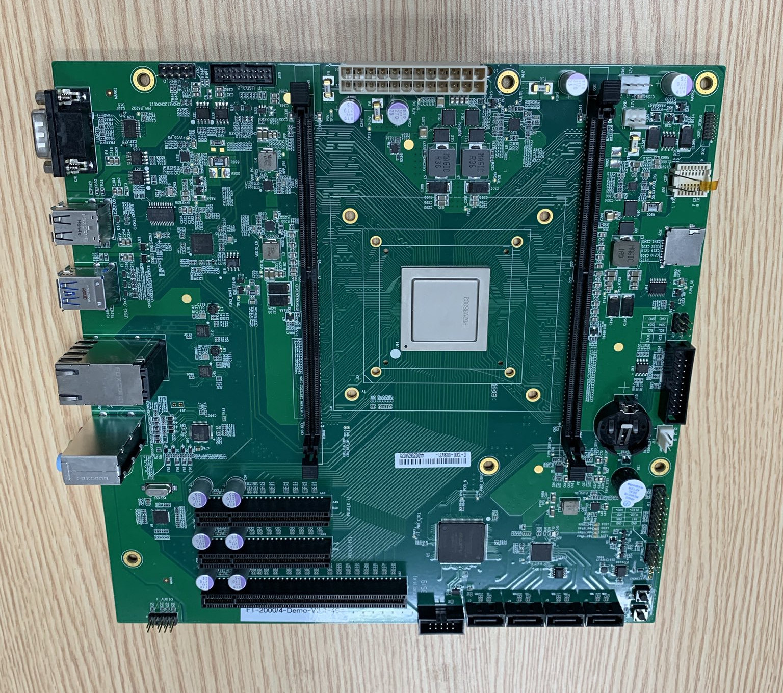
Here are the specifications we derive from the Tweet and the photo:
- SoC – Phytium FT2000/4 quad core custom Armv8 (FTC663) desktop processor @ 2.6 – 3.0 GHz with 4MB L2 Cache (2MB per two cores) and 4MB L3 Cache; 16nm process; 10W power consumption; 1144-pin FCBGA package (35×35 mm)
- System Memory – 2x SO-DIMM slot supporting 72-bit (ECC) DDR4-3200 memory
- Storage – 4x SATA 3.0 connectors; MicroSD card slot
- Video Output – N/A – Discrete PCIe graphics card required
- Audio – Combo jack with 3x 3.5mm port, audio header
- Networking – 2x Gigabit Ethernet ports
- USB – 2x USB 3.0 ports, 2x USB 2.0 ports, 1x USB 3.0 interface via header and 2x USB 2.0 interfaces via header
- Expansion – 1x PCIe x16 and 2x PCIe x8 slots, various pin headers
- Misc – RS-232 serial port, RTC with battery, buzzer, buttons
- Power Supply – ATX connector
- Dimensions – 244 x 244 mm (Micro-ATX form factor)

That’s about all we know about the “FT-2000/4 Demo” motherboard so far, but if you want to know more about the processor check out last month’s announcement (in Chinese), where you’ll also find documentation (still in Chinese) after scrolling a bit.
Basically Phytium FT-2000/4 is an Armv8 desktop processor which consumes up to 10 Watts (3.8W at 1 GHz), and achieves 61.1 and 62.5 points in respectively SPEC2006 integer and the floating-point benchmarks.
The company further explains the desktop PC version of “Galaxy Kirin” operating system (is that Ubuntu Kylin?) has been ported to the processor, and other companies have also been involved in software development. Manufactures such as Lenovo, Baolongda, Lianda, Chuangzhicheng, EVOC, Hanwei and others are developing FT-2000/4-based desktops, notebooks, and all-in-one PC that will launch in Q4 2019 onwards. So we should probably watch that space.

Jean-Luc started CNX Software in 2010 as a part-time endeavor, before quitting his job as a software engineering manager, and starting to write daily news, and reviews full time later in 2011.
Support CNX Software! Donate via cryptocurrencies, become a Patron on Patreon, or purchase goods on Amazon or Aliexpress. We also use affiliate links in articles to earn commissions if you make a purchase after clicking on those links.

Great investigation work on the chip, Jean-Luc! I spent a good deal of time yesterday in vain attempts at figuring out what this chips was.
If you look on the documentation page @ http://phytium.com.cn/Support/index
They have other models including FT2000+/64 with 64x Armv8 cores @ 2.0~2.3GHz.
It’s described as a “High Performance General Purpose Microprocessor”
At the moment I see ARM workstations as mostly aimed at developers, who spend a lot of their time compiling. Having only 4 ARM cores, even good ones, is not going to make it a more interesting machine than what the regular developer CPU like i7-9700 (8 cores at 3 to 4.7 GHz) can bring for ~$300. At least the clearfog brought 16 cores to help.
At least it has gigabit ethernet. Will be interesting to see if those DIMM sockets will accept any old modules from Amazon.
While honeycomb* bringing 16 cores @ 2GHz + DIMMS is a welcome offer, what was mainly missing so far in arm dev world, IMO, was reasonable CPU perf + PCIe availability + SBSA — something that macchiatobin attempted, but largely failed at the PCIe & SBSA departments.
* clearfog got renamed.
TIL: Putting a bog standard ARM SoC on a massive board makes it desktop class.
Phytium makes server chips. It can be argued that this does not necessarily make it a good WS chip, but that’s not a standard ARM SoC.
especially considering the rare ARM cores we see reaching 3 GHz 🙂
while most “desktop” class CPUs are turboing at 4GHz or more.
Ryzen Zen2 can retire 16 instructions per cycle per core. Apple’s Twister closely matches Zen2 clock for clock in single threaded performance.
Phytium 663 can retire 4 instructions per cycle per core, to put things in perspective.
This won’t set any world benchmarking records but it’s not terrible. It’s performance is similar to a Xeon E3-1220 V1 or i3-2100. You can get real work done on it.
If you need an ARM target to run your code on, this isn’t a terrible product, but I’d recommend you look at 96Boards Snapdragon products since those will run circles around this at the same price.
>You can get real work done on it.
I think even if that is true getting real work done on this thing would be far slower and more painful than doing it on an old core 2 duo laptop.
SATA doesn’t seem to be native, but rather via a third party PCIe controller. The same appears to be true for USB 3.0.
There a socket for what appears to be SPI flash, much like a BIOS chip socket on a regular PC motherboard.
FT2000/4 is a 4-year-old core. In that time there’s no public reviews, benchmarks, or community. Either there’s a very forceful embargo in place by the company, or nobody bought it. Probably a bad mix of both.
“Kirin” is most likely an intentional misuse of HiSilicon’s trademark A73-derived product, to create search traffic and fool ignorant readers who will see the name and feel trust without understanding the reference in context.
That’s a common low-end-chinesium product marketing tactic.
You’re thinking of FT-1500A/4 (https://en.wikichip.org/wiki/phytium/feiteng#FT-2000)
No. FT2000/64 was released as a “supercomputing” chip early 2016. FT2000/4 is a low-end part intended for sample implementations.
http://vrworld.com/2016/08/29/china-now-leads-server-race-meet-phytium-mars-processor/
Maybe they have made some changes since then. At the time they talked about “FTC661” cores, but the current processor comes with “FTC663” cores.
I believe they’re still 4-way ARMV8 cores with enhanced streaming SIMD.
Hisilicon Kirin are ARMV9 A73 cores which are much faster clock for clock.
Somebody needs to smack them for inappropriate namedropping to elevate their marketing.
There’s still zero public benchmarks, reviews, or community. That says a lot.
If they want to elevate their credibility, they should put boards in the hands of Anandtech, Phoronix, Tom’s, STH, and CNX, instead of misusing competitor trademarks.
ARMv9? Not quite. A73 is an ARMv8.0 core.
Sorry, ARMV8-A
> instead of misusing competitor trademarks.
Who is doing this? On these CPUs some modified Ubuntu called Kylin can run: http://www.kylinos.cn/news_show.aspx?id=2880 (containing with Kydroid the ability to run Android apps on these ARM thingies)
That article repeats what I posted. There are no evidences of a 10W “2000/4” part back in 2016. There are evidences of a 15W “1500A/4” part from 2016 @ 28nm.
I got it from here: https://translate.google.com/translate?hl=en&sl=zh-CN&u=https://xueqiu.com/8800458425/133199302
“On September 19th, Tianjin Feiteng officially released the newly developed desktop processor FT-2000/4. The performance of this product reached a new high. It is the highest frequency, the lowest power consumption, the latest technology, and the leading cache. A CPU product for desktop terminals.
The most advanced FT-2000/4 processor in China has reached the mainstream CPU level in 2016.”
But it’s a misquote by the site. They mean the 2019 part in comparison to Intel Skylake 2016.
So yes, my bad, this is a 2019 part.
It’s still ARMv8 with a 4-way back end but they’ve improved the memory bandwidth, increased the NEON unit throughput about 30%, shrunk the process 50%, and upped the frequency about 30% from the 662 variants. I can’t find anything about its L1 cache, branch prediction, OOO depth etc.
The 661 arch had 4ALU+2FP dispatch, 32/32KL1, 2ML2 shared between 4 cores, additional 2ML3 per core (must be victim mode) 4 decoders, OOO but no mention of depth or rename buffer size, no mention of TLB size, TAGE branch predictor but no mention of its cache size, no mention of any uOP cache.
661: 50+ pipeline stages, 4 clock L1 cache load latency, operand and stride detection prefetch, in-order retirement, 160 entry ROB, 3-cycle FMUL and FADD, 6-cycle FMA, effectively 8 step NEON queues for each of the 4 ALU and FP units.
50+ pipeline stages? Surely a typo? Perhaps 15?
“160 ISN ROB; 210+ ISN in-flight”. 210/4-issue = 52+ pipeline stages. Even if we only consider filling the ROB alone and forget all other latency mitigation inputs to the formula for picking the pipeline depth – there’s 160 entries. You’d never come close to filling that with a 4 instruction issue unless you have a 50 stage pipeline, and that’s assuming at least 80% utilisation of of the decoders. Not all code can be that dense. Or I guess you could have a 40 stage pipeline ( = 40×4 = 160 ROB size) and be super optimistic about always decoding and retiring 4 ops every cycle.
Wait, you’re counting the breadth and depth of the pipeline, whereas pipeline stages are counted only towards the depth of the pipeline. Perhaps you meant to say ‘pipeline stations’, not stages. For instance CA72 is a 13-18 (min-max) stage deep pipeline, intel’s CSL is 14-19 (min-max). Deepest intel was Prescott with 31 stages (and that was considered a major design flaw).
Compare Zen1 with 192 ROB, divided by 8 retire units is 24, reported as “19+”
With only 4 decode units it makes sense that they’ll seldom fill the ROB, and it makes sense that some instructions are discarded and don’t need to be retired (branch not taken) So I trust that figure of 19+.
The 663 has 4 decode and 4 retire, and they say they manage 210 instructions in flight. 210 / 4 = 52 cycles. In my book if there’s zero cache misses, zero logic unit resource shortages, zero bubbles due to interdependent operands, then how many cycles it takes to move instructions down the pipeline from load to retire is how long the pipeline is.
Maybe they manage to discard and/or fuse 25% of the instructions and that gets it down to 42. It’s still massive, which hides DDR4 latency but costs energy and loses work when IRQ and exceptions occur.
It also answers the question I really meant to ask…. what’s the single thread integer performance like. Somewhere around SNB i3-2120 at 3.3Ghz I would guess. Which isn’t bad really. That’s close to what SKL-U laptops were delivering in 2016, aka what I am using right now. So it’s probably pretty usable for most developers who aren’t compiling kernels every few minutes. 😉
Ok, I see where the confusion comes from. Here’s the thing about ROBs — they are a measure of the breadth of the execution part of the pipeline, but also, and more importantly, of the ‘out-of-orderness’ of the pipeline. A uop may spend way more than a single cycle in the ROB, until all its pre-conditions are met — ie. normally until its predecessor uops get retired. So the higher the OoO-ness of the pipleline, the larger the ROB needs to be, all other things (incl pipeline breadth) considered equal
Take zen1, for instance — the execution engines that directly fill up that 192-entry buffer are not 192 / 8 = 24 stages-deep, they’re 1-7 stages-deep (IIRC), while the front of the pipeline is much narrower – decoder is 4 ops, while dispatcher ‘blows up’ at 10 uops. Finally, the retire unit fed by the ROB is ‘only’ 8 ops/clk.
A more ‘drastic’ example would be intel HSW — 192-entry ROB, can retire 4 ops/clk. Pipeline is not 48-stages deep but 14-19 stages deep, thanks Great A’Tuin ; )
To help visualize things, here’s the CA72 pipeline: https://pc.watch.impress.co.jp/img/pcw/docs/699/491/4.jpg — it’s has 128-strong ROB , and the execution engines are 1-6 stages deep.
So the fact ftc663 has a 210-entry ROB means the design has a fairly high degree of OoO-ness, not that it’s ultra-deep.
I get what you’re saying, but you don’t seem to get what I’m saying, lol.
Maybe you can propose how when there’s 210 instructions in flight and 4 in-order retirement units, the next instruction to be loaded can take the 15 cycles you suggested this core will take to retire all 211 instructions. Are you suggesting that 3.5 instructions on average can be fused for retirement?
No it doesn’t fuse 3.5 instructions. And you’re clearly not getting what I’m saying. So let me rephrase it:
An OoO pipeline may be, e.g. 5 stages deep, and have 200 instructions in flight. Why? Because an instruction may be sitting for hundreds clocks in the ROB, while new instructions are being decoded and dispatched through the pipeline. Consider the following pseudo-code:
ld rn, [address]
mov rx, 42
..
mov ry, 42
(mov repeated 199 times, and the entire sequence is in a ROB of 200 entries)
The first op cache-misses, which will keep the rest of the ROB from retiring for the duration of the latency from main ram — hundreds of cycles.
The ROB is nothing but a measure of the (OoO) window of the pipeline into the instruction stream. The pipeline itself is still 5 stages deep.
I get that the uarch calls it a 5 stage pipeline, but once the ROB is full it becomes impossible for the uarch to process the next loaded instruction in less than 52 cycles without some black magic. Instruction goes in, no cache misses, no bubbles, 52+5 cycles pass before the instruction is retired, minimum. Calling that a 5 stage pipeline is disingenuous, if technically accurate. That is the point you are ignoring over and over. I’m happy to agree that the uarch designer will call it somewhat less.
It’s what blu explains. It’s just a queue in which the control unit can pick any waiting instruction. This is particularly important when combined with branch prediction because this is what allows to fetch one or the other and be able to pick the right one in the least number of cycles possible.
You should not confuse this with latency added to processing an instruction. In fact all instructions get a high latency but you don’t care, what matters is that a large enough number of instructions following the current one have already been prefetched and are ready to be picked there. If you perform an unpredicted jump, you just flush this queue and start to fill it again. But it doesn’t take 50 cycles, it starts executing immediately with an empty queue, thus less opportunities for reordering, and during the time spent executing instructions, others are fetched to refill the queue. So there’s really no added time, it’s just that instructions are executed much longer after they were fetched, but in reality they were fetched much way earlier than needed, “just in case”.
The fact that the vendors expose this metric is because it’s an indication of complexity : being able to instantly pick the most optimal instruction out of 192 possible candidates is nothing trivial at all.
Hoping this helps.
For 663 the only changes I can find are layout (2 cores per L2 instead of 4) and cache differences (L2/L3 effectively doubled because there’s half as many cores per cluster, otherwise same specs, L1 remains at 32/32k) and of course the process shrink, clock rise, NEON throughput improvement, and the memory bus jump from DDR3-1600 to DDR4-3200. The TAGE branch predictor works very well with DDR4 as implemented by AMD for Zen2 so the extra DDR4 latency shouldn’t prevent it from realising near double memory performance.
There’s no mention of any cycle improvements or dispatch/decode/execute/retire width changes in the pipeline. Given the other changes it should still be scaling to about 1.8x FP and memory performance per core, and about 1.4x higher for INT, than the 661 series. If they improved the branch predictor hit rate it could be higher, but I think they would mention improvements if they’d made any.
No use google Chrome and brute force translate the CNX linked Chinese pages to English ( took two attempts on my A95 F2 ), they talk about the new chip and changed features.
Yeah I read them but they don’t go into the the core microarch in any detail.
While I heartily welcome the idea of ARM desktops… using googles automatic translation on the page reveals some interesting things:
“CPU-based built-in security can provide a fundamental and reliable security base for system security. Feiteng proposes a proprietary processor security platform architecture standard PSPA (Phytium Security Platform Architecture), which defines the software and hardware implementation specifications related to Feiteng chip security. The FT-2000/4 supports the PSPA standard and supports the SM2, SM3, and SM4 national secret algorithms to implement trusted computing from the CPU level and effectively escort information security.”
While the FT-2000/4 processor apparently supports the ARMv8 instruction set, it sounds as if there are some extra “proprietary” hardware bits in there to handle platform security and some form of trusted computing. Is this a seperate core/processor?
I’ve not used TEE or such on ARM personally so I may misunderstand a few things.
FT-2000/4 Processor Data Sheet-V1.1 shows that there is a hardware block inside the “System/Security” chunk for the SM2/SM3/SM4/SM9 & TRNG functionality. I can’t read Chinese but Google translate can do a passable job … so section 3.1.1 talks about TEE… 3.1.2 talks about Trusted Boot… “FT-2000/4 built-in Xingen, through the national secret acceleration engine, the system firmware is checked step by step, which realizes the trusted startup and hardware” not clear if that’s a replacement of TEE, or just using different algorithms.. ?
Section 3.1.3 talks about Keys … “Interest security. The FT-2000/4 mainly involves three types of keys: the Feiteng key, the whole machine manufacturer key, and the user key.
The Feiteng key is injected by Feiteng and used by PBR and PBF, and the whole machine manufacturer key is injected by the whole machine manufacturer.
Used, the user key is injected and used by the user. Different keys have their own generation, storage, access, and
Use equal permissions and need to be combined with the life cycle of the chip.”
So this chip has an embedded crypto key management system embedded in it and controlled by the manufacturer?
And 3.1.4 refers to a crypto storage
And 3.1.5 Firmware.. “The PBF firmware is maintained by Feiteng.”
3.1.6 shows that this chip is designed to prevent intrusion
So I wonder how much this system will allow CoreBoot and real Linux security… given the underlying hardware based security will be controlled in China?
No worse than it being controlled in USA or EU. Not quite as bad as it being controlled in Australia.. if you’ve been following the news.
Australia has passed legislation mandating government backdoors in all encrypted communications.
I’m not sure how they plan to enforce that, but it’s doomed by design so no good can possibly come of it, and the poor citizens are at the mercy of idiots who believe they are enforcing something good on their people… which is heart-shreddingly sad because the best of the type of people who aspire to those positions will probably commit suicide when they realise the magnitude of their error, and the worst of them will rape and pillage the economy and rights of the people, in the name of the security of the people, and under the guise of “protection”. Sounds like Mafia? It is Mafia, in legislated, invisible, all-pervasive form.
This is the same setup used almost everywhere. You get access to the machine once the trusted stuff is setup and can load whatever kernel you like. The issue is do you trust the trusted components supplied by the vendor that can’t be replaced.
And we never know that, even with Open Hardware, because there’s no oversight in manufacturing unless we make it ourselves. So we have to accept whether we trust our supplier(s), open or not, partisan or not. If we choose not to trust them, then we need to be fully honest with ourselves about who and what and WHY we do trust another, instead of fooling ourselves that partisan or open = trustworthy, when the blind trust we put in manufacturing affects all camps equally. Here I mean the manufacture of each individual component, not the assembly workers of the final product. Ie if the USB host controller of your mobo has spyware in it, it can use DMA to PWN your memory and that’s the same as handing them root login. If you want a truly trustworthy computer, build yourself a Magic-1. 😉
Best of all, consider how many other far juicier targets there are in the world. Until the criminals have harvested the low-hanging and tasty fruit, they won’t bother with you.
If you’re Jeff Bezos, be very justifiably afraid.
I wouldn’t trust any vendor but I trust random Chinese companies using the state mandated special ciphers less than the rest of them. Knowing what their Linux ports look like I wouldn’t expect their signing etc to actually work properly anyways.