
PCB manufacturing services are pretty cheap and fast nowadays. But imagine some kind of highly transmissible virus hits the globe, somehow the whole global economy shuts down, and you are stuck alone at home with nothing but a Lexmark laser printer. What can you do? Well, you can make your own PCBs! No paper involved.
That’s exactly what Vítor Barbosa did by converting a Lexmark E460(DN) laser printer into a PCB making machine, not because of COVID-19, but instead, because of the price and delays of ordering PCBs in Brazil.
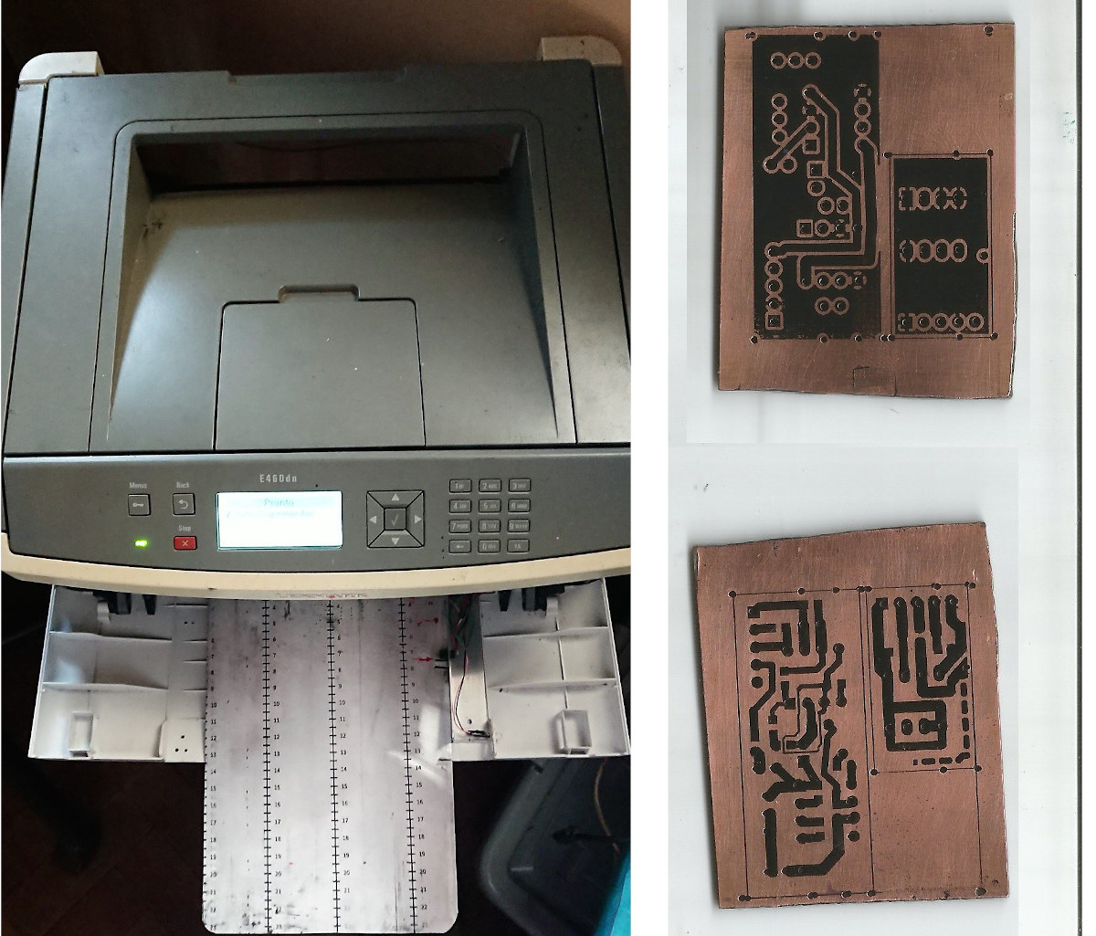
Using a laser printing to make your own PCB like take some work, notably to strip the printer of unused parts such as the fuser and fit it with Arduino Nano or Pro Mini board, an aluminum guide, some resistors and more. The modifications are all explained on Hackaday.io, and this is not a new idea as the project was derived from a 5-year project based on a Lexmark E260, and Haxmark project relying on Lexmark E360D.
Once you are done, you’ll be able to print single or double-layered PCBs directly on copper clad boards with Vítor claiming the resolution is much better than with UV dry film methods, and the system can also print solder masks when combined with a laminator.
You’ll need to print at 1200DPI native resolution to avoid timings issues and “paper” jams, and configure your printer to use the maximum toner amount. A PPD (PostScript Printer Description) is provided in the instructions, and you may want to use it to reproduce the printing conditions on your side. Here’s a quick demo.

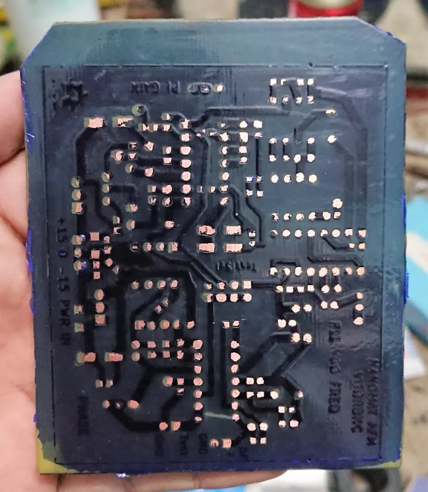
This just shows the printing part, but there are more steps in the process called “Direct Laser Printing” (DLP). After printing, you may want to use acetone vapor to fix the toner to the copper for a couple of minutes, then air dry it for a few seconds before submerging the board into an etchant (Muriatic Acid/Hydrogen Peroxide) for a little while, then finally strip the toner with acetone, and you’re done. A board can be made into about 15 minutes. The video below shows the full process with Lexmark E260.

Via Hackster.io

Jean-Luc started CNX Software in 2010 as a part-time endeavor, before quitting his job as a software engineering manager, and starting to write daily news, and reviews full time later in 2011.
Support CNX Software! Donate via cryptocurrencies, become a Patron on Patreon, or purchase goods on Amazon or Aliexpress. We also use affiliate links in articles to earn commissions if you make a purchase after clicking on those links.


>But imagine some kind of highly transmissible virus hits the globe, somehow the whole global economy shuts down,
FWIW Everything from China has been delayed during the plague but I’ve ordered a few different pcbs from OSHPark including weirder ones like flex and they’ve turned up pretty quickly.
But you don’t live in Brazil I take it? Have you even tried shipping something to Brazil? It’s not like shipping something to most countries, I can tell you that from experience. Only worse place to ship to is Israel.
Some 3 years ago I’d agree with you, but for the past 3 years or so I’ve been getting my parcels from China here in Brazil in a couple weeks to a month depending on shipping method, and that seems to be the norm in most countries.
Uh, try shipping anything into Russia. It’s a sheer lottery.
Cool, looks much faster than my method using the laser engraver ( https://wtarreau.blogspot.com/2019/09/quick-and-clean-pcbs-for-week-end.html ), and probably achieves pretty similar precision. It gets even faster when using few tracks since there’s no need to remove the paint in the void areas, instead you just don’t draw them.
By the way I really don’t understand why they remove the fuser then “emulate” it using acetone vapors. It’s not explained in the article.
Good Idea! Some finetuning & better spezialized toner. Last month some used a cnc craving machine.
Meh. No offense, but… much as I’m interested in all DIY projects around PCB making, my impression is that:
• the resolution in the image shown on the haxmark page (link in article) seems rather lousy
• the PCB examples shown all seem to be for rather large pitch components (which incidentally mostly happen to be those components that you can more easily prototype on a breadboard)
• So it really looks worse than the toner transfer method or than printing a translucent UV exposure mask and going the added step of the classic homemade photosensitive PCB DIY process. AND it requires to mess around with the laser printer’s guts.
I’m more impressed by the DIY projects that use laser diodes to direct expose PCBs
There are some other YouTube videos of this exact same model Lexmark printer making PCBs, and the resolution looks good to me. Here’s an example:
https://youtu.be/5FWUul62irY?t=325
For me that’s not a good example. If I want to make PCBs for PTH components, the resolution I have with the pencil is usually enough. I want a very fine resolution to make circuits for small SMD components. The smallest I’ve done myself was for µSOP (0.65mm pitch), and I expect to be able to route tracks between SOIC pins (1.27mm pitch, 0.15mm track), typically like here: https://1.bp.blogspot.com/-_1oAs1YsqDg/Xq8ssqXxI8I/AAAAAAAABWA/-WJe5MMGJTswDYQmsBOjpWS_QOQrVWs5ACLcBGAsYHQ/s1600/IMG_9762cs.JPG or here: https://1.bp.blogspot.com/-XX0p9k7mOK0/XYe3ayLl4zI/AAAAAAAABF8/LUnLNSbuVXgYSM3B7iaH26jL3cKSCVfHACLcBGAsYHQ/s1600/IMG_8760c.JPG and I’m not anymore convinced based on these videos that the same resolution can be achieved.