
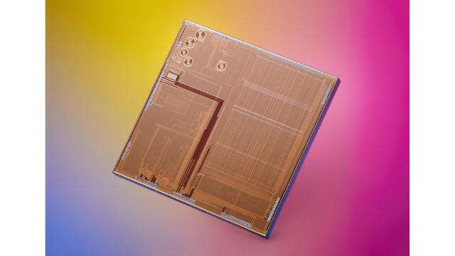
CSEM and USJC together have developed an ultra-low-power RISC-V chip for electronic gadgets such as wearables. The semiconductor companies, from Switzerland and Japan respectively, have been in the market for a while, developing technologies for low-power chips. Their latest collaboration uses Adaptive Body Biasing (ABB) and Deeply Depleted Channel (DDC) to build an ultra-low-power RISC-V chip with all the required and necessary components.
Originating from the labs of CSEM, the Adaptive Body Biasing dwells into the operating efficiency of all the modes of ON, Standby, and OFF. There has been the problem of power leakage in Standby and OFF operating modes, but the Adaptive Body Biasing technology helps design to minimize power leakage when the processor is not operating while keeping the best performance in ON mode.
For most of the designs, the processor is in Standby mode waiting for the incoming data or the next event to be offered. At such times there is a significant amount of power leakage that might reduce the performance of the chip. Adaptive Body Biasing used to design this ultra-low-power chip reduces the amount of power leakage in these periods. With the limited resources available at the moment, EENews Europe have claimed the power consumption to be as low as 10µA in slow mode (see below), and in standby mode, the consumption is about 1pW/bit.
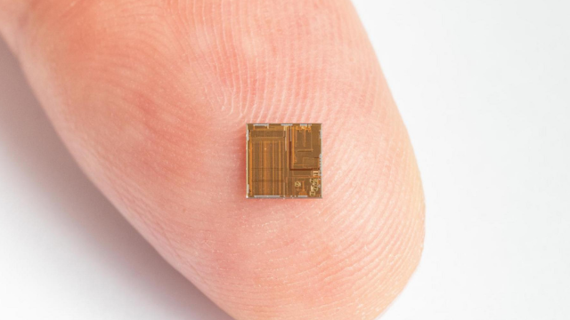
The system-on-chip operates at a threshold voltage of 0.6V and is built with 55nm C55DDC process technology. The ultra-low-power chip features the icyflex-V RISC-V core with an integrated 256KB RAM and 4KB ROM. A technical report published in 2019 by the CSEM scientist tells us more about the ultra-low-power processor based on RISC-V Architecture. This 4-stage pipeline architecture implements the RV32IMC ISA that supports compressed instructions and multiplications.
Coming back to the newly developed RISC-V chip support mode switching in real-time that helps to maintain power efficiency along with performance. The system-on-chip has the capability of coexisting various versions of low-power (for slow and retention modes) and high-speed (for fast mode). More details provided by EENews Europe tell us that the SoC is by default in slow mode at 50 kHz and can be switched to fast mode at 8 MHz. The most awaited parameter, the power consumption by the SoC is 10 µA for the slow mode and 250 µA for the fast mode. In the time of inactivity, the chip is observed to consume about 1µA at the always-on 32KHz clock.
If you are interested in the press release, please visit the CSEM press room page.

Abhishek Jadhav is an engineering student, RISC-V Ambassador, freelance tech writer, and leader of the Open Hardware Developer Community.
Support CNX Software! Donate via cryptocurrencies, become a Patron on Patreon, or purchase goods on Amazon or Aliexpress. We also use affiliate links in articles to earn commissions if you make a purchase after clicking on those links.


It’s a wireless chip as well, but no details about the standard that I could find. I remind me of Ambiq Applo Blue chips like https://www.cnx-software.com/2020/09/17/ambiq-apollo-4-mcu-3%C2%B5a-mhz/ that also use sub-threshold voltage.
Indeed, Apollo4 consumes the same at 3 MHz as this chip at 50 kHz. And at 8 MHz it even consumes 10 times less than this new chip. Anyway at these power levels it becomes possible to build tiny light-powered devices. Think about our good old calculators only relying on a tiny solar panel for example. We can easily imagine some always-on devices with 1cm squared solar sensor as the energy source, that possibly uses radio once in a while from a slowly charged capacitor.
I’m wondering if the need for ultra-low-power in wearables and IoT will bring germanium back, with its 50% lower voltage threshold and higher mobility that may result in an even lower consumption. It’s not suitable for high currents but that’s exactly what we don’t need here.
The docs at https://ambiq.com/apollo4/ suggest the core clocks between 96 and 192MHz, im not sure if it allows low clocking at 3MHz.
No offense, but some of the recent articles look like they come straight from a marketing department.
It’s a restatement of a press release targeting it for the web site’s audience. I found it helpful. I would have liked to see a bit more context added like Jean-Luc did with his comment, but as part of the article.
I would like to rectify, the CSEM is a Swiss company, not east asia…
Since P = 1/2*C*V*V*F:
at 8MHz the power is 250uA
at 32KHz the power is 1uA
since “1/2”, C and V are the same (article did not mention lowering V), you can quickly compare the ratios between the 2 situations:
32000 8000000 32 8000
——— = ————- => — = ——- which is equivalent
1x 10^-6 250 x 10^-6 1 250
So the power reduction is purely from the much lower frequency. IMO: this article does not show how Adaptive Body Biasing that is part of the C55DDC process aids in reducing leakage. A much better comparison would have been to process the same chip with and without ABB. This direct comparison would have shown the impact of ABB which might be fantastic or a ‘dud’.
Now the write up on the C55DDC process is a completely different proof. It does compare two designs (assuming same designs on a similar process node (ie 55nm that is not a high power or medium power process. It should be a 55nm LP process). So this is a far better comparison that the metrics stated in this article.
“East Asia” also intrigued me and I find out it is Japan and Switzerland. I would have preferred the two Nations mentioned than “East Asia”.
While I get the low power market and built to costs of this chip, they should design one with much more ROM. When you think of the complex machine code programs a ZX Spectrum 8 bit could do. A 32 bit device like this could do many low power device needs.
I expect the 4kb program flash is intended for a boot loader, and you would use external flash for the real application, maybe copying it into ram after checking a signature.
I don’t understand this article. Too many buzzwords per line.
What is the bottomline, in normal CNX language?
Ambiq may have RISC-V competition in the future.
As far as I know CSEM is a Swiss company based in Europe and not east asia
Well if you go far far east from asia you will eventually end up in CH…