
Earlier today, I published a review of JeVois-A33 machine vision camera, noting that processing is handled by the four Cortex A7 cores of Allwinner A33 processor, but in the future we can expect such type of camera to support acceleration with OpenCL/Vulkan capable GPUs, or better, Neural network accelerators (NNA) such Imagination Tech PowerVR Series 2NX.
HiSilicon already launched Kirin 970 SoC with such similarIP, except they call it an NPU (Neural-network Processing Unit). However, while looking for camera SoC with NNA, I found a list of deep learning processors, including the ones that go into powerful servers and autonomous vehicles, that also included a 8K Camera SoC with a dual core CNN (Convolutional Neural Network) acceleration engine made by Hisilicon: Hi3559A V100ES.
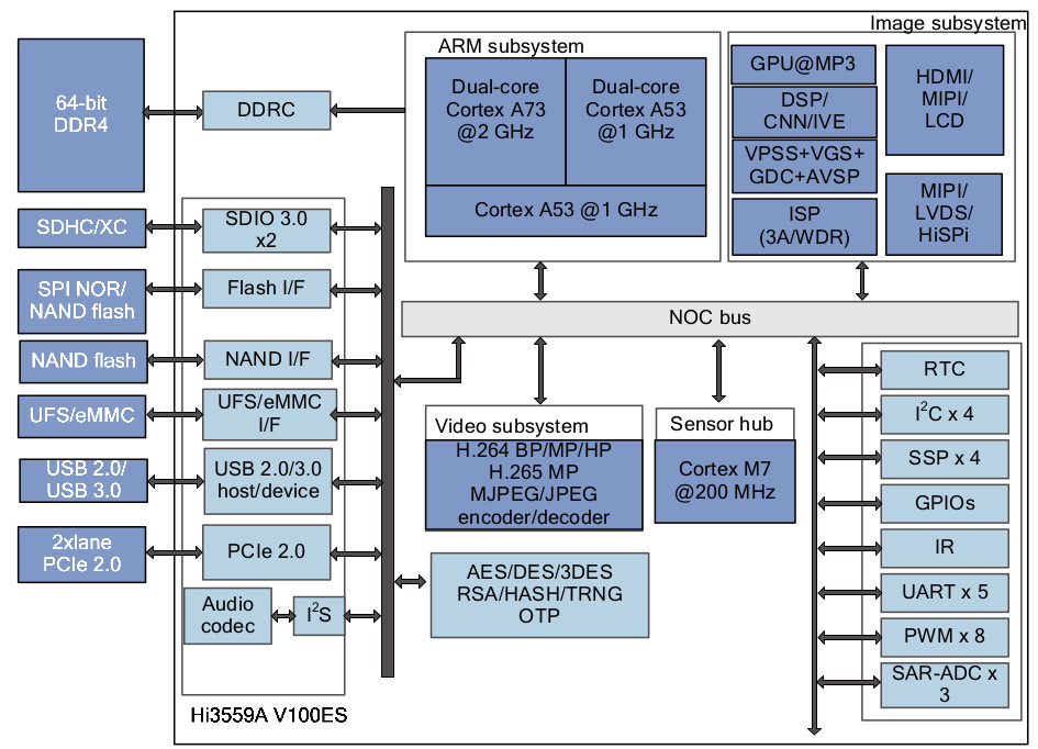
Hisilicon Hi3559A V100ES specifications:
- Processor Cores
- 2x ARM Cortex A73 @ 2 GHz, 32 KB I cache, 64KB D cache or 512 KB L2 cache
- 2x ARM Cortex A53 @ 1 GHz, 32 KB I cache, 32KB D cache or 256 KB L2 cache
- 1x single core ARM Cortex A53 @ 1 GHz, 32 KB I cache, 32KB D cache /128 KB L2 cache
- Neon acceleration and integrated FPU
- GPU – Triple core ARM Mali-G71 GPU@ 900 MHz with 256KB cache, support for OpenCL 1.1/1.2/2.0, and OpenGL ES 3.0/3.1/3.2
- Sensor Hub
- ARM Cortex M7 @200 MHz
- PMC, which supports only external reset, internal POR
- General peripheral IPs (UART, SPI, I2C, PWM, GPIO,and LSADC)
- 3-channel LSADC, 5x UART interfaces, and 8x PWM interfaces
- Memory Interface – 32-/64-bit DDR4 up to 8GB
- Storage Interfaces – SPI NOR flash up to 512MB, NAND flash, eMMC 5.1 up to 2TB, UFS 2.1 up to 512GB
- Video Encoding – H.264 BP/MP/HP, and H.265 Main Profile/Main 10 Profile up to 7680 x 4320@30 fps+1080p@30 fps+7680 x 4320@2 fps snapshot
- Video Decoding – H.264 BP/MP/HP, H.265 MP/Main 10/High Tier up to 8K@30 fps or H.264/H.265 4K@120 fps
- Intelligent Video Analysis
- Integrated intelligent analysis and acceleration engine, allowing customers to develop intelligent applications targeted for mobile camera products
- Dual-core DSP @ 700 MHz, 32 KB I cache, 32 KB IRAM, or 512 KB DRAM
- Dual-core CNN @ 700 MHz neural network acceleration engine
- Video and Graphics Processing
- 3DNR, image enhancement, and DCI
- Anti-flicker for output videos and graphics
- 1/15.5x to 16x video & graphics scaling
- Horizontal seamless stitching of 2-channel videos, and 360° or 720° panoramic stitching of up to 6-channel videos
- OSD overlaying of eight regions before encoding
- Video graphics overlaying of two layers (video layer and graphics layer)
- 2- channel ISP
- Adjustable 3A functions (AE, AWB, and AF)
- FPN removal
- Highlight suppression, backlight compensation, gamma correction, and color enhancement
- DPC, NR, and 6-DOF DIS
- Anti-fog
- LDC and fisheye correction
- Picture rotation by 90° or 270°; Picture mirror and flip
- HDR10, BT.2020 WCG
- Sensor built-in WDR, 4F/3F/2F frame-based/line-based
- WDR and local tone mapping
- ISP tuning tools for the PC
- Audio Encoding and Decoding
- Voice encoding/decoding complying with multiple protocols by using software
- MP3, AAC, and other audio encoding formats
- Audio 3A functions (AEC, ANR, and ALC)
- Security Engine
- AES, DES, and 3DES encryption and decryption algorithms implemented by using hardware
- RSA1024/2048/3072/4096 signature verification algorithm implemented by using hardware
- SHA1/224/256/384/512 of the HASH and HMAC_SHA1/224/256/384/512 tamper proofing algorithms implemented by using hardware
- Integrated 32-kbit OTP storage space and hardware random number generator
- Video Interfaces
- Input
- Multiple sensor inputs. The maximum resolution is 32 megapixels (7680 x 4320).
- 8-/10-/12-/14-bit RGB Bayer DC timing VI, up to 150 MHz clock frequency
- BT.601, BT.656, and BT.1120 VI interfaces
- Maximum 16-lane MIPI/LVDS/sub-LVDS/HiSPi/SLVS-EC interface for the serial sensor inputs
- Maximum 6-channel video inputs for the serial sensor inputs, supporting various working modes such as 1×16-lane/2×8-lane/4×4-lane/2×4-lane+4×2-lane
- Output
- HDMI 2.0, supporting maximum 4K@60 fps output
- 8-/16-/24-bit RGB digital LCD output, supporting maximum 1920 x 1080@60 fps output
- 4-lane MIPI DSI output, supporting maximum 2.5 Gbit/s per lane frequency
- Input
- Audio Interfaces
- Integrated audio codec, supporting 16-bit audio inputs and outputs
- I2S interface for connecting to the external audio codec
- Dual-channel differential MIC inputs for reducing background noises
- Peripherals
- POR, external reset input,
- Internal RTC
- Integrated 2-channel LSADC
- 5x UART interfaces
- IR interface, I2C interface, SSP main interface, and GPIO interface
- Integrated GMAC, supporting RGMII and RMII
- 2x PWM interfaces
- 2x SD 3.0/SDIO 3.0 interfaces, supporting SDXC
- 2x USB 3.0/USB 2.0 host/device ports
- 2-lane PCIe 2.0 RC/EP mode
- Operating Voltages – 0.8V core voltage, 1.8V I/O voltage, 1.2V DDR4 voltage
- Power Consumption – 2.6 Watts
- Package – 15 x 15 mm with 0.4 mm pitch
Boy, that’s a monster… They should have called it MOACSoC (Mother of All Camera SoCs) 🙂 The main ARM cores are said to run Linux+Huawei LiteOS AMP heterogeneous dual systems, and the company provide a dedicated SDK for the consumer mobile camera, cient for the iOS and Android mobile phones, and a high-
performance H.265 decoding library. The SDK might be in the wild as “Hi3559AV100ES_SDK_V2.0.2.0” but I did not find a download link. I got all information above from Hi3359A V100ES ultra-HD Mobile Camera SoC product brief.
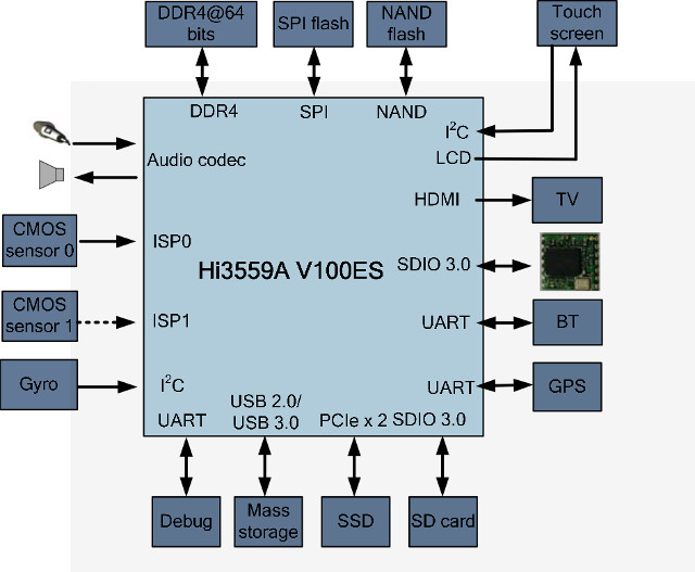
Based on the block diagram above, some mobile camera and professional camera will start taking SSD drives beside the boring SD card and USB 2.0/3.0 storage devices.
Hi3559A V100ES will also be found in drone cameras, 3D/VR cameras, and 4K/8K network-based EDR. I have no idea what the latter stands for, but the photo in the document looks like a car dashboard camera with display. Anyway, this should allows for some interesting use cases with near real-time object recognition.
Hisilicon showcased a dynamic object categorization and identification system at CPSE2017 in Shenzhen earlier this month. The company did not mention Hi3559A V100, but made clear an 8K solution was used.
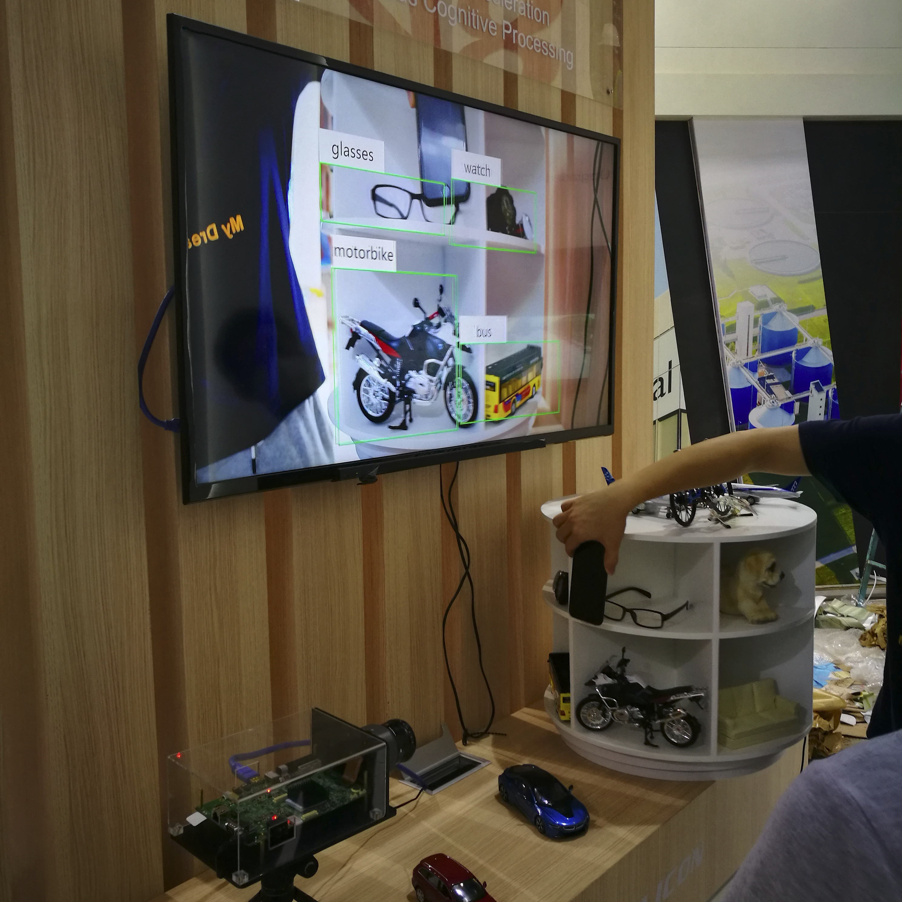
If we are to believe one person on Tencent’s ncnn Github repo, performance is really good with a 10ms lag for GoogleNet, and 89ms for VGG-SSD. We’ll have to wait a little to get more details, and Hisilicon did not post any product info on their website about their new 8K SoC, only about the earlier Hi3559 2K/4K SoC.

Jean-Luc started CNX Software in 2010 as a part-time endeavor, before quitting his job as a software engineering manager, and starting to write daily news, and reviews full time later in 2011.
Support CNX Software! Donate via cryptocurrencies, become a Patron on Patreon, or purchase goods on Amazon or Aliexpress. We also use affiliate links in articles to earn commissions if you make a purchase after clicking on those links.


These chips are cutting edge and cost around $45-50.
Get driver working for free is sweet dream, maybe for next 5 years because autonomous drive car technology segment.
“4K/8K network-based EDR. I have no idea what the latter stands for”
https://en.wikipedia.org/wiki/Event_data_recorder
Has anyone used this chips for their project? It looks like they doesn’t support OpenCV. I wonder how hard it will be to implement something in their own IVE syntax. I am looking forward to see if anyone has used it and how they are using development environment for this.