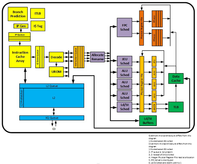
2017 was the year of systems based on Intel’s low power, low cost Apollo Lake processors, and provided Intel does not suddenly decide to cancel yet another product, they will be replaced by Gemini Lake processors in 2018. The former is based on Goldmont microarchitecture, while the latter relies on the updated Goldmont microarchitecture.
Intel has now released a document entitled “Intel 64 and IA-32 Architectures Optimization Reference Manual” where you’ll find more gritty technical details about Goldmont Plus in chapter 16 “SOFTWARE OPTIMIZATION FOR GOLDMONT PLUS, GOLDMONT, AND SILVERMONT MICROARCHITECTURES”.

The enhancements over Goldmont include:
- Widen previous generation Atom processor back-end pipeline to 4-wide allocation to 4-wide retire, while maintaining 3-wide fetch and decode pipeline.
- Enhanced branch prediction unit.
- Improved AES-NI instruction latency and throughput.
- 64KB shared second level pre-decode cache (16KB in Goldmont microarchitecture).
- Larger reservation station and ROB entries to support large out-of-order window.
- Wider integer execution unit. New dedicated JEU port with support for faster branch redirection.
- Radix-1024 floating point divider for fast scalar/packed single, double and extended precision floating point divides.
- Larger load and store buffers. Improved store-to-load forwarding latency store data from register.
- Shared instruction and data second level TLB. Paging Cache Enhancements (PxE/ePxE caches).
- Modular system design with four cores sharing up to 4MB L2 cache.
- Support for Read Processor ID (RDP) new instruction.
We had a discussion a little while ago comparing 64-bit ARM and Intel Apollo Lake OpenSSL benchmark, and Intel was a bit behind for some key sizes, so maybe the new AES-NI improvements in Gemini Lake/Goldmont Plus will bring low power Intel processor back to the front.
The document also contains a table comparing Goldmont Plus and Goldmont’s “Front End Cluster Features”.
| Feature | Goldmont Plus Microarchitecture | Goldmont Microarchitecture |
| Number of Decoders | 3 | |
| Max. Throughput Decoders | 20 Bytes per cycle | |
| Fetch and Icache Pipeline | Decoupled | |
| ITLB | 48 entries, large page support | |
| 2nd Level ITLB | Shared with DTLB | |
| Branch Mispredict Penalty | 13 cycles (12 cycles for certain Jcc) | 12 cycles |
| L2 Predecode Cache | 64K | 16K |
This table shows many similarities, but GLM+ has a bigger 64KB L2 cache, and a larger mispredict penalty (that’s certainly more than compensated by the larger cache). More information can be found in the Intel document.

Jean-Luc started CNX Software in 2010 as a part-time endeavor, before quitting his job as a software engineering manager, and starting to write daily news, and reviews full time later in 2011.
Support CNX Software! Donate via cryptocurrencies, become a Patron on Patreon, or purchase goods on Amazon or Aliexpress


It looks a lot like what I remember of the P3 or Pentium-M, both of which were very efficient CPUs in their time. It’s good to see x86 improving on the low power designs. If at least Atoms can become again as fast as ARM CPUs, we can hope for a more balanced offering depending on expected performance level, power envelope and price. Ie choose between power efficiency and price for a similar performance level, or select between performance and price for a given power envelope.
😮 that 64KB difference with 16KB