
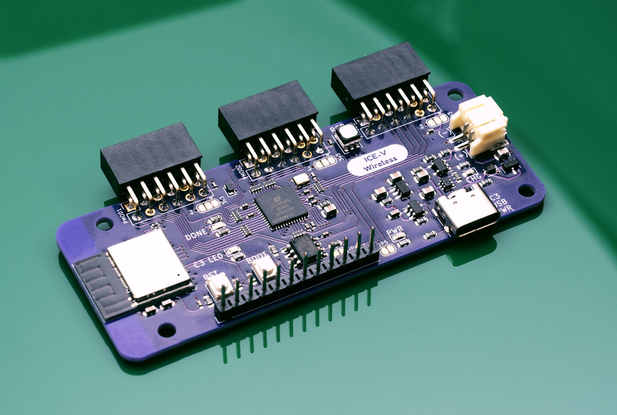
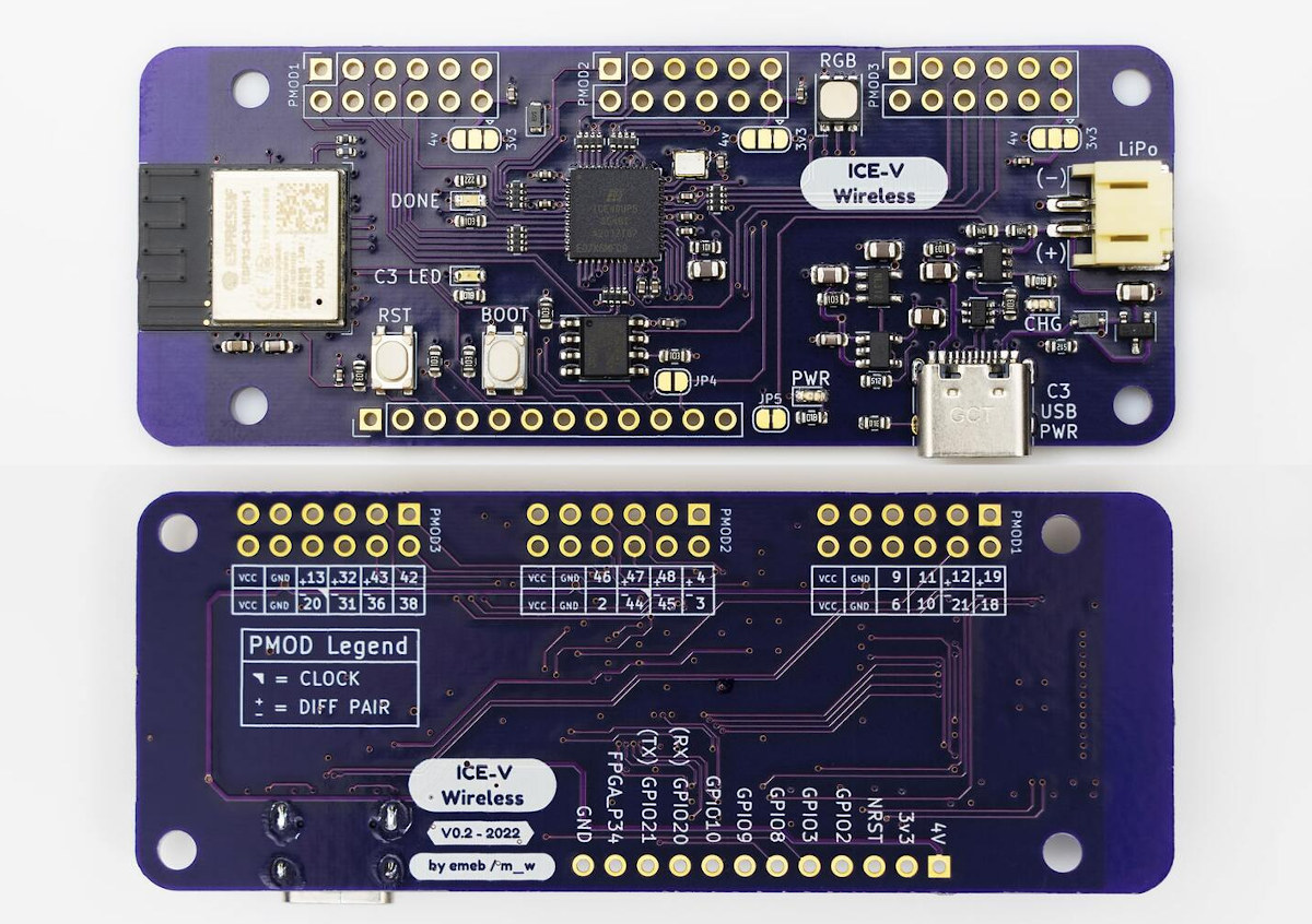
Lattice Semi ICE40 boards are pretty popular notably thanks to the availability of open-source tools. ICE-V Wireless is another ICE40 UltraPlus FPGA board that also adds wireless support through an ESP32-C3-MINI-1 module with WiFi 4 and Bluetooth LE connectivity.
Designed by QWERTY Embedded Design, the board also comes with 8MB PSRAM, offers three PMOD expansion connectors, plus a header for GPIOs, and supports power from USB or a LiPo battery (charging circuit included).
ICE-V Wireless specifications:
- FPGA – Lattice Semi ICE40UP5K-SG48 FPGA with 5280 LUTs, 120 Kbits EBR RAM, 1024 Kbits PSRAM
- External RAM – 8MB PSRAM
- Wireless – ESP32-C3-MINI-1 module with 2.4 GHz WiFi 4 and Bluetooth LE through ESP32-C3 RISC-V processor, 4MB flash.
- USB – 1x USB Type-C port for power, programming, and JTAG debugging of the ESP32-C3 module
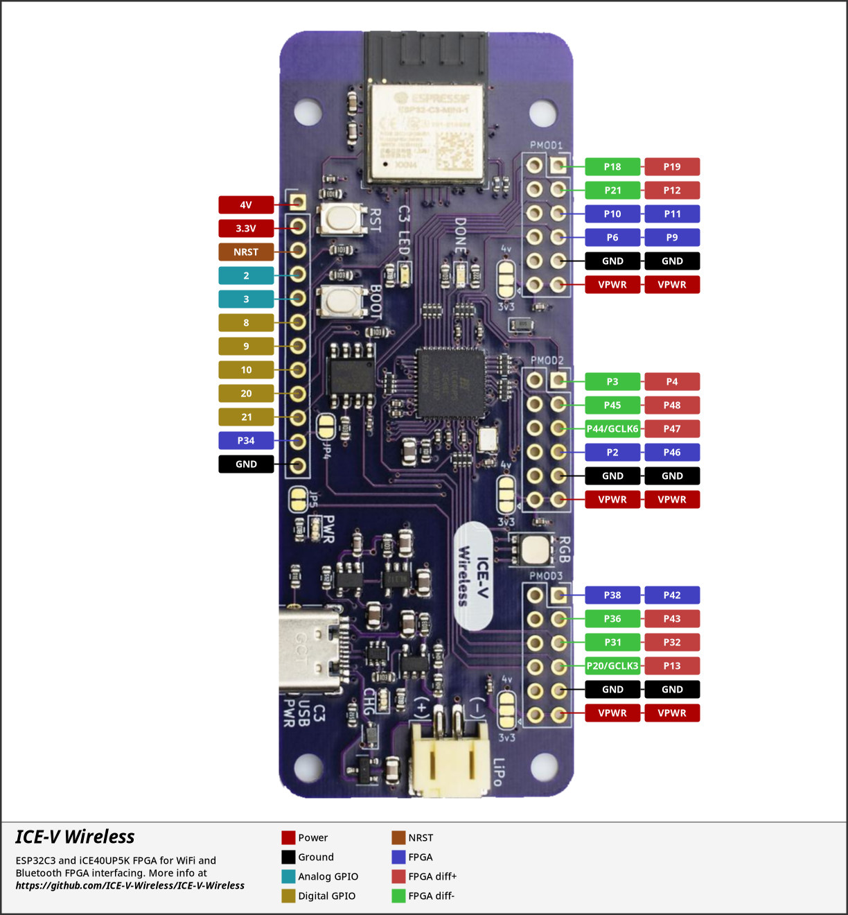
- Expansions
- 3x PMOD connectors connected to the FPGA
- I/O connector with 7x ESP32-C3 GPIO lines (serial, ADC, I2C) and one FPGA line, plus power, ground, and reset.
- Misc – RGB LED, Reset and Boot buttons, various LEDs for power, charging, etc…
- Power Supply
- 5V via USB-C port
- LiPo power/charger
- Dimensions – TBD
The ESP32 firmware is written in C with the ESP-IDF V5.0 toolchain and libraries and provides a TCP socket interface over WiFi that loads the FPGA configuration at powerup from a SPIFFS filesystem contained in the ESP32-C3’s flash, and allows for updates to the FPGA over WiFi (ESP32 and ICE40 are connected through SPI), as well as monitoring of the LiPo battery voltage. The iCE40 FPGA gateware demonstrates basic SPI monitor/control via SPI with a flashing LED. The host computer can control the board through a Python script.
The KiCad 6.0-based hardware design is open-source, and so are the firmware, gateware, and Python script just mentioned, with everything hosted on Github, where you’ll also find some basic documentation.
The ICE-V Wireless FPGA board is now offered on GroupGets for $75 plus shipping with the group buying campaign scheduled to end on August 16, 2022.

Jean-Luc started CNX Software in 2010 as a part-time endeavor, before quitting his job as a software engineering manager, and starting to write daily news, and reviews full time later in 2011.
Support CNX Software! Donate via cryptocurrencies, become a Patron on Patreon, or purchase goods on Amazon or Aliexpress. We also use affiliate links in articles to earn commissions if you make a purchase after clicking on those links.


It’s particularly unclear to me what battery-powered application could benefit from combining an FPGA and a wireless module. There probably are, but isn’t this a tiny niche market ? I’m a bit confused I must confess.
Would it not allow over the air updates and upgrades, reception tunning without changing hardware ?
I don’t know, I still don’t understand who needs that. I mean, OTA updates for anything is fine if this thing needs wireless connectivity in the first place. You probably don’t want a fingerprint reader in the safe burried in your basement to support OTA updates for example (yeah a stupid example, that was to show that some devices do not need this). That’s what still puzzles me.
considering niche markets: really missing a generic (plug&dev) wireless USB 2.0 (IEEE 802.11n/Wifi5) (USB 3.1gen1 (aka 3.0), bandwidth >= IEEE 802.11 ac/ax/Wifi6) hub (?)
Battery usually serves as a secondary power source, like a backup when the primary source (usb-c) is lost or temporarily interrupted. If this board is used in some remote monitoring device it can still operate during power loss, which can be critical for the application.
Small robotics. Audio processing. FPGA learning. I’m sure there are plenty others. Sure it’s niche, but so are a lot of “maker” products.
Hello! We’re helping host the device’s campaign – we used your question for an interview! Thank you for asking your question, and here’s a short snippet of the ICE-V Wireless team answering it. We’ll soon have the full interview posted.
https://twitter.com/groupgetscom/status/1544763026498154496?s=20&t=aIgxpmwTM6ZN9lvn9GYeFA