CNXSoft: This is a guest article by Dave Fohrn, Embedded Software Engineer at Cologne Chip AG, that goes into detail about the company’s open-source integrated logic analyzer (ILA) for GateMate FPGA chips.
A field-programmable gate array (FPGA) is a highly flexible integrated circuit in which complex logic circuits can be configured. They are often used as custom computing units in digital circuits because of their ability to process data quickly and in parallel using individually configured circuits.
The digital circuits designed specifically for FPGAs are usually developed in a hardware description language such as Verilog or VHDL and are known as gateware. The term “gate” refers to the configurable digital logic units in the FPGA on which the individual gate circuits are implemented. An effective design can accelerate the computing process by strategically utilizing the various resources available in the FPGA, processing data in parallel, and intelligent implementing pipelining.
A logic analyzer, a common tool in digital technology, can be used to record and analyze digital signals in electronic circuits. Typically, a logic analyzer is connected to external pins of components such as FPGAs or microcontrollers to record the electronic signal levels at an adjustable sampling frequency. Triggers are defined to capture a specific period of time around a defined event, responding to events such as a change in signal level or the occurrence of a specific signal pattern. After recording all the sampled values around a trigger event, the user can analyze the signal levels in a waveform.
A so-called Integrated Logic Analyser (ILA) is implemented directly as gateware in an FPGA and allows the evaluation of the internal signal waveforms of the gateware to be tested (Design Under Test, DUT for short) directly in the FPGA. The ILA gateware is connected to the DUT signals to be analyzed and configured together with the DUT on an FPGA. This allows developers to monitor the behavior of their gateware’s internal signals under real-world conditions, without affecting the normal operation of the DUT. The duration of DUT signal acquisition around a given trigger event is limited by the hardware resources available in the FPGA. However, with an ILA, a trigger event can be captured for any length of time and repeated as often as required. This provides deep insight to better understand and optimize the functionality of complex systems.
In real-world environments, complex failures often occur that cannot be detected by simulations. Post-implementation timing simulations, which attempt to simulate the gateware as realistically as possible, are extremely computationally intensive and can deviate from reality. Particularly when gateware is operated at the limits of its specification, timing problems and signal integrity degradation are not uncommon. In addition, external factors such as noise and temperature variations can change the behavior of the system. It is also possible that unexpected events occur in the periphery of the FPGA that were not taken into account in the simulation. An ILA can be used specifically to identify such errors, which are difficult to simulate.
Cologne Chip now offers an ILA specifically designed for the GateMate FPGA. The ILA offers a comprehensive set of features to support both the development of Gateware and the implementation of the GateMate FPGA in complex systems.
Gateware
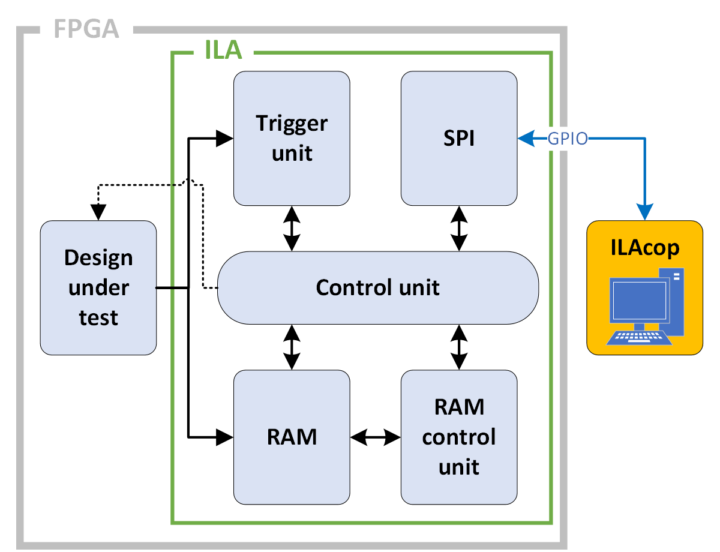
With the components shown in Figure 1, the gateware of the ILA efficiently utilizes a minimal part of the hardware resources available in the FPGA. This allows the ILA to be configured in parallel with a resource-intensive DUT on the FPGA without affecting its normal operation.

The test signals selected by the user are combined into a test vector and connected to both the RAM and the trigger unit. After the test vector has been synchronized by a user-selectable number of register levels, it is sent directly to the data input of the RAM. The ILA’s RAM is flexible in data width and depth and is built in the FPGA from Block RAM cells. In the trigger unit, the test vector is checked for the set trigger condition.
The application software known as ILAcop (ILA control program) is installed on the operating system of the user’s PC and allows both the configuration of the ILA gateware before implementation and the control of the ILA gateware at runtime via the serial peripheral interface (SPI for short). By default, the ILA uses a USB interface for connection to the user’s PC and an FTDI chip for USB-to-SPI translation, which is used both on the Cologne Chip Evaluation Board and in the GateMate programmer adapter for uploading the configuration data stream. This has the advantage that the hardware setup can be used for analysis after the FPGA has been configured without any changes.
The control unit coordinates the communication with ILAcop. It configures the trigger to be set in the trigger unit, holds the DUT in the reset state if necessary, and starts the data acquisition process.
The RAM control unit is responsible for ensuring that the sampled values of the test vector are available for the defined period of time around the set trigger event after the data acquisition. For this purpose, the number of samples before and after the trigger event is calculated and set during the configuration of the ILA gateware based on the set sampling rate and the user-defined recording duration. During sampling, the data logger is in circular buffer mode. After the last cell has been written, the first cell is overwritten. When the trigger is activated, a counter is started which counts the samples up to the required number in parallel with the storage and then finishes the data acquisition process.
After the data acquisition process, the stored samples are read from the RAM and transferred serially to ILAcop via SPI. ILAcop reconstructs the signal waveform from the received data and visualizes it for the user.
Workflow
The entire workflow is controlled by the Python program ILAcop. The first step is to configure the ILA gateware for the individual DUT. Configurations such as the ILA’s clock source, the duration of data acquisition, the activation of desired additional functions, and the selection of DUT signals to be tested can either be made using the configuration wizard or read from a JSON file.

In the next step, the abstractly described gateware of ILA and DUT, which are already interconnected through various signals at this point, will be configured on the FPGA. First, the entire gateware must be synthesized using Yosys, a powerful open-source synthesis tool. During the synthesis process, the circuit is optimized and mapped onto the specific hardware components of the GateMate FPGA.
The placement and interconnection of the circuit elements on the FPGA are then performed by Cologne Chip’s proprietary P&R software. This software is specifically designed for efficient handling of the FPGA layout and generates a configuration file that addresses and configures all hardware elements required for the gateware in the FPGAs.
The final transfer of the configuration data to the FPGA is performed using the OpenFPGAloader, another open-source tool that specifically supports loading configuration files to a large number of FPGA devices.
Once the FPGA has been successfully configured, communication between ILAcop and ILA gateware begins. At runtime, the user can use a terminal to set the trigger conditions, activate and deactivate the reset of the DUT, and start the data acquisition process.
After data acquisition, the stored samples are read from the RAM and transferred serially to ILAcop via the SPI. ILAcop reconstructs the signal waveform from the received data and visualizes it for the user.

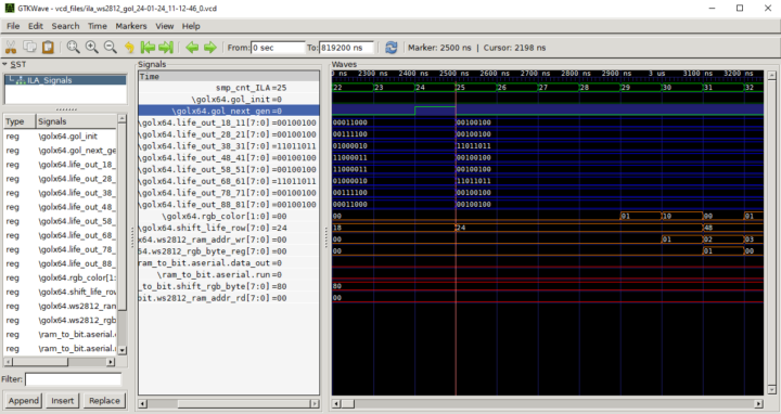
Figure 3 shows a waveform visualized by GTKWave showing the signals of a DUT from the FPGA recorded by the ILA. Alternatively, any other waveform viewer with VCD (Value Change Dump) import can be used. The waveform shown is taken from the example DUT in the Cologne Chip GateMate ILA Repository on GitHub. The complete example including explanations can be found in the repository under “gatemate_ila/example_dut/ws2812_gol/”. The signal names in the timing diagram are made up of the modules in which they are defined, organized hierarchically, and separated by a dot and the original name from the DUT.
Features of the GateMate ILA
- Setup Wizard: The user is guided through the configuration of the ILA to analyze a DUT by an intuitive and easy-to-use shell procedure that provides explanations for all configurations.
- Comprehensive analysis of the DUT source code: The system automatically identifies the DUT’s hierarchy and searches through its modules, saving the names of all signals defined in the design. It also searches for any special GateMate hardware elements used by the DUT, such as PLLs or Block RAMs, and saves them for further processing.
- Flexible and simple selection of a sampling frequency: The sampling frequency can be set by selecting the output of an additional PLL with a user-selectable frequency, an external clock, or a clock defined in the DUT, such as the output of an instantiated PLL.
- Parallel sampling of over 1,000 signals: The DUT signals are selected by the user from a hierarchical list and combined into a test vector. The maximum number of bits in a test vector and the total number of samples that can be stored depends on the available Block RAM cells in the FPGA, i.e. those not used by the DUT. The CCGM1A1 FPGA has 32 Block RAM cells, which are operated with the ILA gateware in true dual-port mode. The number of available addresses and the data bus width are variably configurable. With a test vector width of 5 bits, up to 8,192 sampled values can be stored per Block RAM cell. If, for example, 30 Block RAM cells are available to the ILA, a total of 245,760 sampled values can be stored with a data width of 5 bits. The maximum possible data width of a Block RAM cell is 40 bits, with 1,024 memory addresses available. With 30 Block RAM cells, a test vector can have a maximum width of 1,200 bits, and a total of 1,024 sampled values can be stored.
- Configuration of the ILA from a JSON file: All configurations created by the wizard are stored in a JSON file in plain text format. This allows the user to easily make subsequent changes, such as selecting different signals to analyze. Using the JSON file allows quick and easy configuration of the ILA.
- Trigger reconfigurable at runtime: Using the ILA’s built-in communication interface, the trigger condition can be changed at any time via an interactive shell program from the user’s computer, and the data acquisition process on the FPGA can be started or stopped without affecting the operation of the DUT.
- Reset hold function: This function allows signals to be acquired immediately after the DUT has left the reset state. The DUT reset can be enabled or disabled as required prior to data acquisition, while the reset is disabled as soon as data acquisition is started.
- User-defined bit patterns as triggers: The ILA allows individual trigger events to be defined. A specific bit pattern can be defined in hexadecimal or binary form to be set as the expected trigger event across the entire test vector. Each bit of the pattern can be configured as ‘1’, ‘0’, or ‘X’ (for ‘don’t care’). In addition, a trigger can be set on any signal, triggered by events such as a rising or falling edge of the signal.
- Signal analysis via waveform: Once the defined trigger event has occurred, the waveform of the signals can be analyzed in a waveform viewer using the original names and vector sizes from the DUT in a timing diagram.
- Configuration of data acquisition sequences: Sequences can be created with different trigger conditions that are executed immediately after each other. This makes it possible to record sample values for events that follow each other at short intervals. As soon as the required samples have been received, the next trigger condition starts the recording. Each recording from these sequences is displayed in a separate time diagram.
- Open Source: As an open-source tool, the ILA offers a high degree of flexibility and customization, as well as the opportunity for further development by the community.
ILA configuration example with resource usage overview
The resource consumption of the ILA is variable due to its generic design and depends on the configuration. This includes the functions set by the user, the bit width of the test vector, and the number of samples required.
The DUT has a single clock domain generated by a PLL. This clock domain is set in the configuration of the ILA gateware for storing the samples in order to synchronize the recording process with the DUT. This offers the advantage that the test vector does not need to be synchronized to the ILA recording clock domain before being stored, and no additional signal line of the global clock network is required. In some cases, it may be advantageous to select an additional PLL with a significantly higher frequency, e.g. for performance optimization or to analyze different clock networks and asynchronous processes. However, this will also reduce the maximum possible recording time, as the RAM will be filled more quickly.
The DUT is reset using the CC_USR_RSTN primitive. The CC_USR_RSTN primitive allows the gateware to be temporarily reset immediately after FPGA configuration. The ILA has been configured so that the reset signal of CC_USR_RSTN can also be controlled via the SPI interface, i.e. this signal can be controlled using ILAcop. The function of the CC_USR_RSTN primitive is maintained.
The test was performed on the Evaluation Board V3.1B with a CCGM1A1 FPGA. The CCGM1A1 FPGA has 64 20k-bit RAM blocks and 20,480 CPEs (Cologne Programmable Elements), each with an 8-bit LUT tree for logic functions and two memory elements that can be used as a flip-flop or latch.
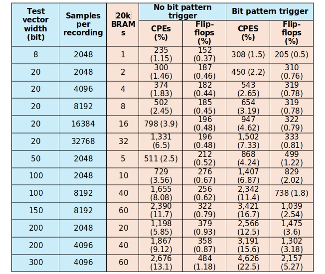
The resource consumption of the ILA on the CCGM1A1 FPGA is shown. Depending on the bit width of the test vector and the number of samples per recording, the consumption of block RAM cells (20k BRAMs), CPEs, and flip-flops is shown. For each configuration, tests were performed with and without user-defined bit patterns as triggers.
The analysis shows a remarkably low resource consumption. For a configuration with an 8-bit test vector and a total of 2,048 samples per acquisition, only 235 CPEs are required, which is 1.15% of the CPEs of the smallest FPGA in the GateMate series. In addition, 152 flip-flops are used, which is only 0.37% of the total flip-flops available.
With the consumption of 60 20k RAM blocks, the ILA has reached the capacity limit of the total RAM blocks available on the FPGA. Without bit pattern triggers, 11.7% of the total CPEs are used with a test vector width of 150 bits and 8,192 samples, and 13.1% with a test vector width of 300 bits and 4,096 samples. It can be seen that the resource consumption is higher when the vector width is increased rather than the number of samples. This becomes even clearer when the bit pattern trigger is enabled: at maximum memory usage, 16.7% of the CPEs are used with a test vector width of 150 bits and 22.5% with a test vector width of 300 bits on the CCGM1A1 FPGA.

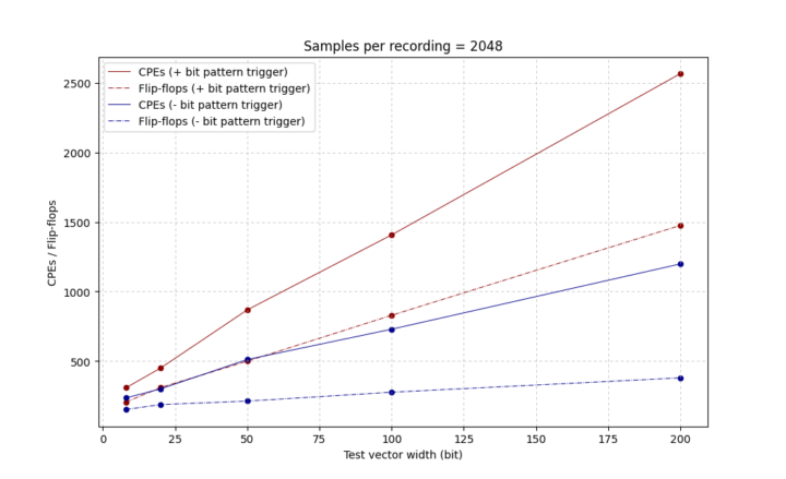
In Figure 5, the test vector width is increased while the number of samples per acquisition remains constant. It can clearly be seen that the hardware consumption increases almost linearly with
increasing test vector width. The hardware consumption increases much more steeply when the bit pattern trigger is enabled.
Conclusion
The GateMate ILA provides developers of gateware for GateMate FPGAs with a useful tool to thoroughly analyze the signals of the design under test in its real working environment. Particularly
noteworthy is the low hardware consumption with minimal configuration, allowing the ILA to be implemented even with very limited hardware resources. Efficient implementation and the use of pipelining techniques minimize the critical path of the ILA gateware. This enables analysis even in high-frequency ranges.
The flexible design, developed as an open-source project, is continually being enhanced with additional features. This makes the ILA even more powerful in supporting the development of custom gateware.
The source code of the ILA gateware and ILAcop, as well as instructions for use and installation, can be found at: https://github.com/colognechip/gatemate_ila

Jean-Luc started CNX Software in 2010 as a part-time endeavor, before quitting his job as a software engineering manager, and starting to write daily news, and reviews full time later in 2011.
Support CNX Software! Donate via cryptocurrencies, become a Patron on Patreon, or purchase goods on Amazon or Aliexpress. We also use affiliate links in articles to earn commissions if you make a purchase after clicking on those links.


People should be more concerned about the market conditions that allow FPGAs evaluation boards to be priced linearly between around 7.5k to around 32k LUTs while products using them end up seeing exponential price increases as it’s an open invitation for Chinese vendors to compete on price point. Open sourcing would mitigate the harm to some extent but when the likes of the Analog Discovery 3 launch for such BoM factors they’re really just asking for it.