
Right after ARM’s Cortex-M7 announcement, STMicro has listed STM32F7 MCU family based on the latest ARM core on their website. The family is comprised of 20 different MCUs with various flash size, packages, and with or without a crypto/hash coprocessor. The company expects their STM32F756xx microcontrollers to be used for motor drive and application control, medical equipment, industrial applications such as PLC, inverters, and circuit breakers, printers & scanners, alarm systems, video intercom, HVAC, home audio appliances, mobile applications, Internet of Things application, and wearable devices such as smartwatches.
STM32F7 MCUs share the following key features:
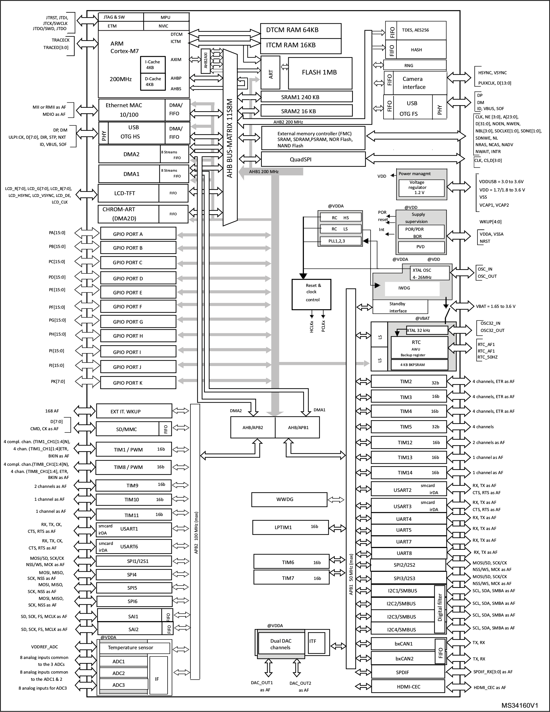
- Cortex-M7 core @ 200 Mhz (1000 CoreMark/428 DMIPS) with L1 cache (4KB I-cache, 4KB d-cache)
- 320KBytes of SRAM with scattered architecture:
- 240 Kbytes of universal data memory
- a 16 Kbytes partition for sharing data over the bus matrix
- 64 Kbytes of Tightly-Coupled Data Memory (DTCM) for time critical data handling (stack, heap…)
- 16 Kbytes of Tightly-Coupled Instruction Memory (ITCM) for time critical routines
- 4 Kbytes of backup SRAM to keep data in the lowest power modes.
- 512 to 1024 KB flash memory
- AXI and multi-AHB bus matrix for interconnecting Core, peripherals and memories
- Two general purpose DMA controllers and dedicated DMAs for Ethernet, high-speed USB On-The-Go and the Chrom-ART graphic accelerator.
- Peripheral speed independent from CPU speed (dual clock support) allowing system clock changes without impacting the function of the peripherals
- Other peripherals:
- 2x serial audio interfaces (SAI) with SPDIF output support
- 3x I2S half-duplex with SPDIF input support
- 2x USB OTG with dedicated power supply
- Dual Quad SPI interface
- 3x 12-bit ADC with 16 to 24 channels
- 2x 12-bit DAC with 2 channels
- 2x CAN Bus
- Camera Inteface
- LCD-TFT interface
- GPIOs: 82 to 168 depending on model
- Operating voltage – 1.7 to 3.6V
- Power efficiency:
- 7 CoreMark/mW at 1.8V and 180 MHz
- 120µA typical current consumption in Stop mode with all context and SRAM saved
- Temperature Range:
- Ambient temperatures: –40 to +85 °C /–40 to +105 °C
- Junction temperature: –40 to + 125 °C
As announced this morning Cortex M7 is backward compatible with Cortex M4 instruction set, and to simply upgrades from STM32F4 to STM32F7, ST Micro has made the new F7 series pin-to-pin compatible with F4 series.
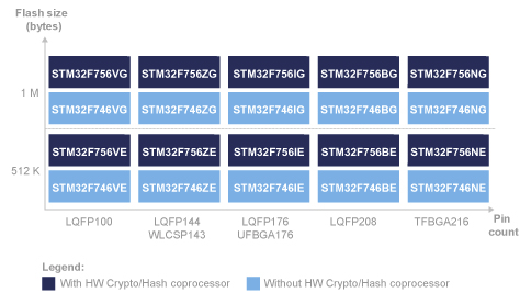
There are 20 models divided into 5 families with the key differences listed in the table below.
| STM32F756Vx | STM32F756Zx | STM32F756Ix | STM32F756Bx | STM32F756Nx | |
| SPI/I2S | 4/3 (simplex) | 6/3 (simplex) | |||
| GPIOs | 82 | 114 | 140 | 168 | |
| ADC Channels | 16 | 24 | |||
| Package | LQLP100 | WLCSP143 LQFP144 |
UFBGA176 LQFP176 |
LQFP208 | TFBGA216 |
If you can read German, and are interested in knowing more about Cortex-M7 and/or STM32F7, you may want to read a long article on Electroniknet including the Cortex-M4 vs Cortex M7 below, that appears to be a bit more detailed than the info on Anandtech, since it includes FPU and power consumption details.
| Property | ARM Cortex-M4 | ARM Cortex-M7 | |
|---|---|---|---|
| ISA | ARMv7M-E | ARMv7M-E | |
| Command length | 16/32 bit | 16/32 bit | |
| Thumb instructions | Thumb-2 | Thumb-2 | |
| Integer pipeline | 3 steps | 6 steps Dual Issue | |
| Memory Architecture | Harvard | Harvard | |
| L1 cache (instructions / data) | No | 4-64 KB / 4-64 KB | |
| TCM (instructions / data) | No | 0-16 MB / 0-16 MB | |
| FPU (single / double precision) | FPv4 Yes / No * | FPv5 Yes / Yes | |
| Floating point register | 32×32 bit | 32×32 bit / 16×64 bit | |
| 32-bit divider | Yes | Yes | |
| Memory protection unit | Optional 8 areas | Optional 16 or 32 areas | |
| System Interfaces | 3xAHB Lite 32 bit | 1×64 bit ITCM, DTCM 2×32 bit, 1xAXI 64 bit, 32 bit 2xAHB Lite | |
| Nested Vectored Interrupt Controller | 1-240 external interrupts | 1-240 external interrupts | |
| Interrupt priorities / NMI | 256 / Yes | 256 / Yes | |
| DMIPS / MHz – Mark Core / MHz (IAR) | 1.25 / 1.52 ** – 3.4 | 2.14 / 2.52 ** – 5.0 | |
| Interrupt latency | 12 clock cycles | 11-12 clock cycles | |
| Power Saving | 3 (Sleep / Deep Sleep / Deep Sleep WIC) | 3 (Sleep / Deep Sleep / Deep Sleep WIC) | |
| Real-time trace | optional only code | optional code and data | |
| Breakpoints / watchpoints | 2-6 / 1-4 | 2-6 / 1-4 | |
| Lockstep operation | No | Yes | |
| Clock rate (maximum) in 40 nm LP | 300 MHz *** | 400 MHz | |
| Power consumption in 90 nm LP | 33 uW / MHz | 53 uW / MHz # | |
| Power consumption in 40 nm LP | 8 uW / MHz | 12.9 uW / MHz # | |
| Announcement | February 2010 | September 2014 | |
Back to STM32F7. Currently only STM32F756NF is listed, and the marketing status is set to “preview”, so the MCU is only available to “lead” customer for now, and it will be demonstrated at ARM Techcon 2014 next week. I could not find any information about a development board (Discovery / Nucleo) either. You can find more information including STM32F7 datasheet on the STMicro STM32F7 Series page. For a quick overview of the capabilities and performance of STM32F7, you may also want to read that 23-page presentation.

Jean-Luc started CNX Software in 2010 as a part-time endeavor, before quitting his job as a software engineering manager, and starting to write daily news, and reviews full time later in 2011.
Support CNX Software! Donate via cryptocurrencies, become a Patron on Patreon, or purchase goods on Amazon or Aliexpress

Hi
512 to 1024 MB flash memory should be 512 to 1024 kB flash memory. ie. kB not MB.
Keep up the great work.
Kind regards
Jimmy