PADI IoT Stamp module powered by Realtek RTL8710AF ARM Cortex M3 WiFi SoC is a potential competitor to Espressif ESP8266 modules. Pine64, the manufacturer of the module, sent me their kit with a $2 IoT stamp, a breakout board, a USB to TTL debug board and a J-Link debug board. In the first part of the review I’ve shown the hardware and how to assemble PADI IoT stamp kit. In the second part I’m going to write a tutorial / getting start guide showing how to control the board with AT commands, build the firmware with GCC SDK, and finally demonstrate how to flash and debug the firmware with the J-Link debugger.
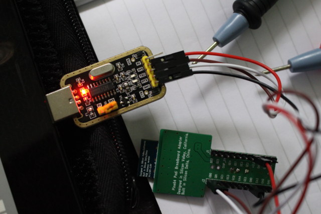
The Quick Start Guide indicates you need to connect the USB to TTL debug board to UART2 instead of UART1 as I did on the very similar B&T RTL-00 RTL8710AF module, and set connection settings to 38400 8N1. This did not work for me, and I had indeed to connect the USB to TTL board to UART0 instead (GB0 & GB1 pins).

I’ll be using a Ubuntu 16.04 (Linux) computer for this quick start guide, but you can work with Windows and Mac OS X too, as tools as available for all three operating systems. So in my case I configure minicom to 38400 8N1 using /dev/ttyUSB0 device, and the boot log is almost the same as B&T RTL-00 with the same ROM version and toolchain:
|
1 2 3 4 5 6 7 8 9 10 11 12 13 14 15 16 17 18 19 20 21 22 23 24 25 26 27 28 29 30 31 32 33 |
# ATSR ========================================================= ROM Version: 0.3 Build ToolChain Version: gcc version 4.8.3 (Realtek ASDK-4.8.3p1 Build 2003) ========================================================= Check boot type form eFuse SPI Initial Image1 length: 0x3a78, Image Addr: 0x10000bc8 Image1 Validate OK, Going jump to Image1 BOOT from Flash:YES ===== Enter Image 1 ==== load NEW fw 0 Flash Image2:Addr 0xb000, Len 287564, Load to SRAM 0x10006000 No Image3 Img2 Sign: RTKWin, InfaStart @ 0x10006079 ===== Enter Image 2 ==== #interface 1 is initialized interface 0 is initialized Initializing WIFI ... Start LOG SERVICE MODE # WIFI initialized init_thread(53), Available heap 0xc840 AT_UART_CONF: 38400,8,1,0,0 RTL8195A[HAL]: ISR 81 had been allocated!!! [GPIO Err]HAL_GPIO_Irq_Init: GPIO Pin(0) Unavailable |
There are however some changes, and for example the firmware used on PADI IoT Stamp has slightly more heap available. The guide also mentions ATS? should show all command available, but it’s not working for me:
|
1 2 3 4 5 6 |
# ATS? [MEM] After do cmd, available heap 60656 # |
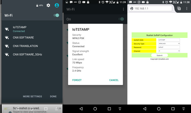
Typing “help” as I did with RTL-00 module does not work either, and that does not look since documentation appears to be wrong again, but that’s not a big deal since we have all AT commands listed in that document. I could configure it as “IoTSTAMP” access point:
|
1 2 3 4 5 6 7 8 9 10 11 12 13 14 15 16 17 18 |
#ATPW=2 [MEM] After do cmd, available heap 55584 # ATPA=IoTSTAMP,wifiiot2,3,0 Writting boot mode 0x77665502 and Wi-Fi setting to flash ... LwIP_DHCP: dhcp stop. Deinitializing WIFI ... WIFI deinitialized Initializing WIFI ... WIFI initialized [MEM] After do cmd, available heap 55584 # |
and enable the HTTP server with ATSW AT command:
|
1 |
#ATSW=c |
It rebooted the IoT stamp with the same WiFi setting, and I could connect to its demo web page for configuration.

Since everything is so similar to B&T RTL-00 I’ll just point out to the post “Getting Started with B&T RTL-00 RTL8710 Module – Serial Console, AT Commands, and ESP8266 Pin-to-Pin Compatibility” for more tests with different AT commands. I still tried to turn on and off the a GPIO pin using the ATSG command since it’s something I did not do with RTL-00:
|
1 2 3 4 5 6 7 8 9 10 11 12 13 14 15 16 |
#ATSG=W,GC_0,1,1,0 [ATSG]: _AT_SYSTEM_GPIO_CTRL_ PORT: GC_0[32] DIR: 1 PULL: 0 [MEM] After do cmd, available heap 60656 # ATSG=W,GC_0,0,1,0 [ATSG]: _AT_SYSTEM_GPIO_CTRL_ PORT: GC_0[32] DIR: 1 PULL: 0 [MEM] After do cmd, available heap 60656 |
The first line pull GC0 pin to high level (3.3V), while the second command brings it down to low level (0V). Details about ATSG command:
|
1 |
ATSG=R/W,Pin_number,data (0|1), direction (0: input | 1: output), and pin mode (0: PullNone/PullDefault | 1: PullUp | 2: PullDown | 3: OpenDrain) |
I did not connect an LED, but instead measured the value with multimeter and could confirm the voltage level was right in both cases.
B&T provided an SDK which required a an unlicensed / pirated version of IAR ARM Workbench, but Pine64/Realtek have released a GCC SDK that do you require you to use pirated software. You can download sdk-ameba-rtl8710af-v3.5a_without_NDA_GCC_V1.0.0 (198 MB) directly from Pine64 website. After unzipped the SDK you can enter sdk-ameba-rtl8710af-v3.5a_without_NDA_GCC_V1.0.0 directory, and open readme.txt to have a look at RTL8710 GCC SDK structure:
|
1 2 3 4 5 6 7 8 9 10 11 12 13 14 15 16 17 18 19 20 21 22 23 24 25 26 27 28 29 30 31 32 33 34 35 36 37 38 39 40 41 42 43 44 45 46 47 48 49 50 51 52 53 54 55 56 57 58 59 60 61 62 63 64 65 66 67 68 69 70 71 72 73 74 75 76 77 78 79 80 81 82 |
########################################################################################### ########################################################################################### ####################RTL8710_GCC_VERSION_V1.0.0############################################# ########################################################################################### GCC SDK RTL8710 basic version (including the window platform cygwin installation and Ubuntu platform Linux Installation routines), including cross compilation of the installation, compile, link, run, debug, and so on. SDK implementation of the function: 1, WiFi connection settings (including AP mode and STA mode). 2, peripheral resource control (including GPIO, SPI, UART, IIC, etc.). 3, the user uses the sample method. SDK directory is as follows, please first read the document: UM0096 Realtek Ameba-1 build environment setup - gcc.pdf ├── component │ ├── common │ │ ├── api │ │ ├── application │ │ ├── drivers │ │ ├── example │ │ ├── file_system │ │ ├── mbed │ │ ├── network │ │ ├── test │ │ └── utilities │ ├── os │ │ ├── freertos │ │ └── os_dep │ └── soc │ └── realtek ├── doc │ ├── AN0004 Realtek low power wi-fi mp user guide.pdf │ ├── AN0011 Realtek wlan simple configuration.pdf │ ├── AN0012 Realtek secure socket layer(ssl).pdf │ ├── AN0025 Realtek at command.pdf │ ├── AN0033 Realtek Ameba-1 over the air firmware update.pdf │ ├── AN0038 Realtek googlenest user guide.pdf │ ├── AN0043 Realtek mdns user guide.pdf │ ├── AN0045 Realtek Ameba-1 power modes.pdf │ ├── AN0046 Realtek Ameba uart adapter.pdf │ ├── AN0049 Realtek Ameba WiGadget iot demo kit application note.pdf │ ├── AN0075 Realtek Ameba-1 at command v2.0.pdf │ ├── UM0006 Realtek wificonf application programming interface.pdf │ ├── UM0014 Realtek web server user guide.pdf │ ├── UM0023 Realtek Ameba-1 build environment setup - iar.pdf │ ├── UM0027 Realtek Ameba-1 crypto engine.pdf │ ├── UM0034 Realtek Ameba-1 memory layout.pdf │ ├── UM0039 Realtek Ameba-1 SDK quick start.pdf │ └── UM0096 Realtek Ameba-1 build environment setup - gcc.pdf ├── project │ └── realtek_ameba1_va0_example │ ├── example_sources │ ├── GCC-RELEASE │ ├── inc │ └── src ├── release_note.txt └── tools ├── arm-none-eabi-gcc │ ├── 4.8.3-2014q1 │ ├── 4.8.3-2014q1.tar.gz │ └── gcc-arm-none-eabi-4_8-2014q1-20140314-linux.tar.bz2 ├── autopatch │ └── auto_patch.bat ├── DownloadServer │ ├── DownloadServer.exe │ ├── readme.txt │ └── start.bat ├── file_check_sum │ └── file_checksum.c ├── iperf.exe ├── serial_to_usb │ └── mbedWinSerial_16466.zip ├── simple_config_wizard │ ├── Android │ └── iOS ├── simple_config_wizard_3.4b │ ├── Android │ └── iOS ├── uart_adapter │ └── app └── wigadget ├── Android └── iOS |
Since I only aim to write a getting started guide I won’t go through all of it, but we can see the low level source code & binary, some documentation, an example project, and some tools include Android and iOS apps, OTA download server and more.
Nevertheless the readme.txt tells us to first read “UM0096 Realtek Ameba-1 build environment setup – gcc.pdf” in order to setup our development environment. The instructions are available with Windows and Linux, but again I’m only test them using Ubuntu 16.04. They’ll be very similar since you’ll rely on cygwin in Windows, and if you run the latest Windows 10 you should be able to install Windows subsystem for Linux, and use the Linux instructions.
First you have to make sure some tools and libraries are installed:
|
1 |
sudo apt install build-essential gawk bc libc6-dev:i386 lib32ncurses5-dev |
then we can build the sample project:
|
1 2 |
cd project/realtek_ameba1_va0_example/GCC-RELEASE/ make |
If everything goes well the log should end showing “Image manipulating” as follows:
|
1 2 3 4 5 6 7 8 9 10 11 12 13 14 15 16 17 18 19 20 21 22 23 24 25 26 27 28 29 30 31 32 33 34 35 36 37 |
=========================================================== Image manipulating =========================================================== ../../../tools/arm-none-eabi-gcc/4.8.3-2014q1/bin/arm-none-eabi-nm application/Debug/bin/application.axf | sort > application/Debug/bin/application.nmap ../../../tools/arm-none-eabi-gcc/4.8.3-2014q1/bin/arm-none-eabi-objcopy -j .image2.start.table -j .ram_image2.text -j .ram_image2.rodata -j .ram.data -Obinary application/Debug/bin/application.axf application/Debug/bin/ram_2.bin ../../../tools/arm-none-eabi-gcc/4.8.3-2014q1/bin/arm-none-eabi-objcopy -j .sdr_text -j .sdr_rodata -j .sdr_data -Obinary application/Debug/bin/application.axf application/Debug/bin/sdram.bin cp ../../../component/soc/realtek/8195a/misc/bsp/image/ram_1.p.bin application/Debug/bin/ram_1.p.bin chmod 777 application/Debug/bin/ram_1.p.bin chmod +rx ../../../component/soc/realtek/8195a/misc/iar_utility/common/tools/pick ../../../component/soc/realtek/8195a/misc/iar_utility/common/tools/checksum ../../../component/soc/realtek/8195a/misc/iar_utility/common/tools/padding ../../../component/soc/realtek/8195a/misc/iar_utility/common/tools/pick 0x`grep __ram_image2_text_start__ application/Debug/bin/application.nmap | gawk '{print $1}'` 0x`grep __ram_image2_text_end__ application/Debug/bin/application.nmap | gawk '{print $1}'` application/Debug/bin/ram_2.bin application/Debug/bin/ram_2.p.bin body+reset_offset+sig b:268460032 s:268460032 e:268759452 size 299420 copy size 299420 ../../../component/soc/realtek/8195a/misc/iar_utility/common/tools/pick 0x`grep __ram_image2_text_start__ application/Debug/bin/application.nmap | gawk '{print $1}'` 0x`grep __ram_image2_text_end__ application/Debug/bin/application.nmap | gawk '{print $1}'` application/Debug/bin/ram_2.bin application/Debug/bin/ram_2.ns.bin body+reset_offset b:268460032 s:268460032 e:268759452 size 299420 copy size 299420 ../../../component/soc/realtek/8195a/misc/iar_utility/common/tools/pick 0x`grep __sdram_data_start__ application/Debug/bin/application.nmap | gawk '{print $1}'` 0x`grep __sdram_data_end__ application/Debug/bin/application.nmap | gawk '{print $1}'` application/Debug/bin/sdram.bin application/Debug/bin/ram_3.p.bin body+reset_offset b:805306368 s:805306368 e:805306368 size 0 copy size 0 ../../../component/soc/realtek/8195a/misc/iar_utility/common/tools/padding 44k 0xFF application/Debug/bin/ram_1.p.bin total 44 k, padding data ff, name application/Debug/bin/ram_1.p.bin Original size 15032 Padding size 45056 cat application/Debug/bin/ram_1.p.bin > application/Debug/bin/ram_all.bin chmod 777 application/Debug/bin/ram_all.bin cat application/Debug/bin/ram_2.p.bin >> application/Debug/bin/ram_all.bin if [ -s application/Debug/bin/sdram.bin ]; then cat application/Debug/bin/ram_3.p.bin >> application/Debug/bin/ram_all.bin; fi cat application/Debug/bin/ram_2.ns.bin > application/Debug/bin/ota.bin chmod 777 application/Debug/bin/ota.bin if [ -s application/Debug/bin/sdram.bin ]; then cat application/Debug/bin/ram_3.p.bin >> application/Debug/bin/ota.bin; fi ../../../component/soc/realtek/8195a/misc/iar_utility/common/tools/checksum application/Debug/bin/ota.bin || true size = 299436 checksum 1ce5dfe rm application/Debug/bin/ram_*.p.bin application/Debug/bin/ram_*.ns.bin make[1]: Leaving directory '/media/hdd/edev/realtek/iotstamp/sdk-ameba-rtl8710af-v3.5a_without_NDA_GCC_V1.0.0/project/realtek_ameba1_va0_example/GCC-RELEASE' |
We can find the application in application/Debug/bin directory:
|
1 2 |
ls -l application/Debug/bin/ram_all.bin -rwxrwxrwx 1 jaufranc jaufranc 344492 Nov 26 14:37 application/Debug/bin/ram_all.bin |
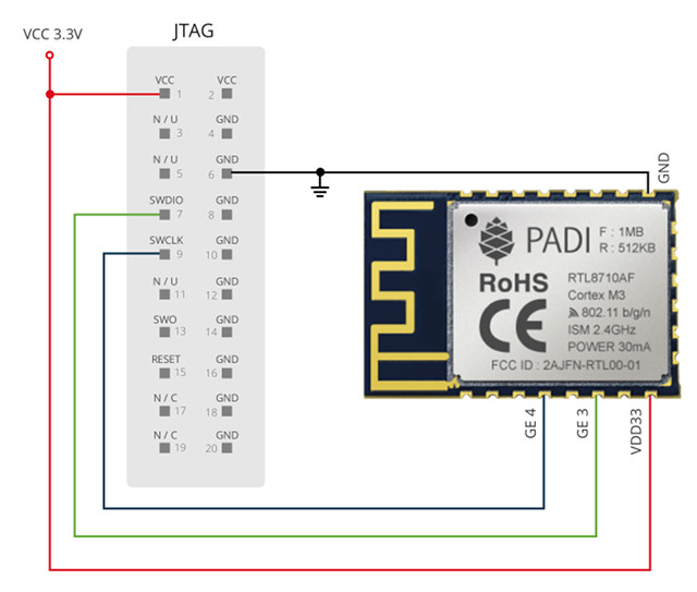
There’s also an ota.bin image which might be usable using OTA firmware update documentation, but for this guide I want to use the J-Link debugger that the company sent me instead. The GCC SDK is not for PADI IoT stamp, but instead for Realtek Ameba Arduino board, and you’ll be asked to connect the board through one of the micro USB port. That won’t work with IoT stamp since there’s no USB port at all, and instead you’ll need to go and back forth between multiple documentation, and connect the board as per the JTAG/SWD connections diagram shown below.
 That document also mentions that:
Required external power VCC 3.3V, JTAG/SWD didn’t supply power to the PADI IoT Stamp, VCC connection from PADI IoT Stamp is used by JTAG/SWD as voltage reference only.
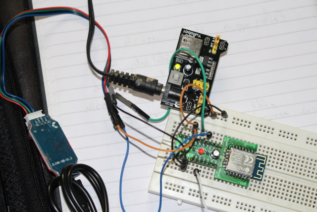
At first, I did not see that, and used it without external power supply, but since I was not successful with the J-Link debugger (for another reason), so I ended up inserting PADI IoT stamp into a breadboard and added Ywrobot power board to provide an external 3.3V power source.

I also soldered a 22uF capacitor, since I’ve read it’s not optional, as it may affect WiFi connection due to power issue. Once I complete the wiring, I connected the debugger to my computer:
|
1 2 3 4 5 6 |
[13822.997460] usb 1-1.1: new full-speed USB device number 5 using ehci-pci [13823.111841] usb 1-1.1: New USB device found, idVendor=1366, idProduct=0101 [13823.111854] usb 1-1.1: New USB device strings: Mfr=1, Product=2, SerialNumber=3 [13823.111860] usb 1-1.1: Product: J-Link [13823.111864] usb 1-1.1: Manufacturer: SEGGER [13823.111869] usb 1-1.1: SerialNumber: 000000123456 |
There are two sets of instructions in UM96 document to download and flash the code: OpenOCD/CMSIS-DAP and JLink, so since I had a J-Link debugger, I went with that latter. First you have to download J-Link Software and Documentation pack and for my system I selected ” Linux, DEB Installer, 64-bit V6.12″. After accepting the EULA, I got JLink_Linux_V612_x86_64.deb file which I installed as follows:
|
1 |
sudo dpkg -i JLink_Linux_V612_x86_64.deb |
Now we can start JLink GBD server for a Cortex-M3 as explained in the document:
|
1 2 3 4 5 6 7 8 9 10 11 12 13 14 15 16 17 18 19 20 21 22 23 24 25 26 27 28 29 30 31 32 33 34 35 36 37 38 39 40 41 |
/opt/SEGGER/JLink/JLinkGDBServer -device cortex-m3 SEGGER J-Link GDB Server V6.12 Command Line Version JLinkARM.dll V6.12 (DLL compiled Nov 25 2016 18:02:55) -----GDB Server start settings----- GDBInit file: none GDB Server Listening port: 2331 SWO raw output listening port: 2332 Terminal I/O port: 2333 Accept remote connection: yes Generate logfile: off Verify download: off Init regs on start: off Silent mode: off Single run mode: off Target connection timeout: 0 ms ------J-Link related settings------ J-Link Host interface: USB J-Link script: none J-Link settings file: none ------Target related settings------ Target device: cortex-m3 Target interface: JTAG Target interface speed: 1000kHz Target endian: little Connecting to J-Link... J-Link is connected. Firmware: J-Link ARM-OB STM32 compiled Aug 22 2012 19:52:04 Hardware: V7.00 S/N: 20090928 Feature(s): RDI,FlashDL,FlashBP,JFlash,GDBFull Checking target voltage... Target voltage: 3.30 V Listening on TCP/IP port 2331 Connecting to target...ERROR: Could not connect to target. Target connection failed. GDBServer will be closed...Restoring target state and closing J-Link connection... Shutting down... Could not connect to target. Please check power, connection and settings.jaufranc@CNX-LAPTOP3:~$ |
So the JLink debugger is detected, but failed to connect to the target. Apart from the last error, everything looks exactly as in the documentation. That’s when I started to add an external power boar, solder the capacitor, and double check my connection. But finally after many trials and errors, I realized that I had to use a SWD connection (SWCLK/SWDIO signals) instead of JTAG…
|
1 2 3 4 5 6 7 8 9 10 11 12 13 14 15 16 17 18 19 20 21 22 23 24 25 26 27 28 29 30 31 32 33 34 35 36 37 38 |
/opt/SEGGER/JLink/JLinkGDBServer -device cortex-m3 -if swd SEGGER J-Link GDB Server V6.12 Command Line Version JLinkARM.dll V6.12 (DLL compiled Nov 25 2016 18:02:55) -----GDB Server start settings----- GDBInit file: none GDB Server Listening port: 2331 SWO raw output listening port: 2332 Terminal I/O port: 2333 Accept remote connection: yes Generate logfile: off Verify download: off Init regs on start: off Silent mode: off Single run mode: off Target connection timeout: 0 ms ------J-Link related settings------ J-Link Host interface: USB J-Link script: none J-Link settings file: none ------Target related settings------ Target device: cortex-m3 Target interface: SWD Target interface speed: 1000kHz Target endian: little Connecting to J-Link... J-Link is connected. Firmware: J-Link ARM-OB STM32 compiled Aug 22 2012 19:52:04 Hardware: V7.00 S/N: 20090928 Feature(s): RDI,FlashDL,FlashBP,JFlash,GDBFull Checking target voltage... Target voltage: 3.30 V Listening on TCP/IP port 2331 Connecting to target...Connected to target Waiting for GDB connection... |
Now keep the GDB server running, open a new terminal windows in the same directory (where you’ve built the code), and run make flash to download and flash the code to the board:
|
1 2 3 4 5 6 7 8 9 10 11 12 13 14 15 16 17 18 19 |
make flash .... Breakpoint 2, RtlFlashProgram () at rtl_flash_download.c:524 524 in rtl_flash_download.c FILEENDADDR$340 = 0x54000 Restoring binary file ./application/Debug/bin/ram_all.bin into memory (0x10022fc8 to 0x10023174) Breakpoint 2, RtlFlashProgram () at rtl_flash_download.c:524 524 in rtl_flash_download.c dump for check start addr of dumping$341 = 0x98000000 end addr of dumping$342 = 0x980541ac Breakpoint 3: file rtl_flash_download.c, line 556. Breakpoint 3, RtlFlashProgram () at rtl_flash_download.c:556 556 in rtl_flash_download.c make[1]: Leaving directory '/home/jaufranc/edev/realtek/iotstamp/sdk-ameba-rtl8710af-v3.5a_without_NDA_GCC_V1.0.0/project/realtek_ameba1_va0_example/GCC-RELEASE' |
There will be a lot of message as above, and the GDB Server windows will show its own set of messages:
|
1 2 3 4 5 6 7 8 9 10 11 12 13 14 15 16 17 18 19 |
... Reading 8192 bytes @ address 0x9804A000 Reading 8192 bytes @ address 0x9804C000 Reading 8192 bytes @ address 0x9804E000 Reading 8192 bytes @ address 0x98050000 Reading 8192 bytes @ address 0x98052000 Reading 428 bytes @ address 0x98054000 Read 2 bytes @ address 0x1000225C (Data = 0xF649) Read 2 bytes @ address 0x1000225E (Data = 0x7BB4) Read 2 bytes @ address 0x10002260 (Data = 0x2238) Read 2 bytes @ address 0x10002262 (Data = 0xF2C1) Read 2 bytes @ address 0x100025BC (Data = 0xBF00) Setting breakpoint @ address 0x100025BC, Size = 2, BPHandle = 0x0157 Starting target CPU... Reading all registers Removing breakpoint @ address 0x100025BC, Size = 2 Read 4 bytes @ address 0x100025BC (Data = 0xF898BF00) Reading 64 bytes @ address 0x1FFFFFC0 GDB closed TCP/IP connection |
Now if you want to debug your code, you can run make debug to start the gdb console:
|
1 2 3 4 5 6 7 8 9 10 11 12 13 14 15 16 17 18 19 20 21 22 23 24 25 26 27 28 29 30 31 32 33 |
make debug if [ ! -d ../../../tools/arm-none-eabi-gcc/4.8.3-2014q1 ] ; then tar -jxf ../../../tools/arm-none-eabi-gcc/gcc-arm-none-eabi-4_8-2014q1-20140314-linux.tar.bz2 -C ../../../tools/arm-none-eabi-gcc/ ; mv ../../../tools/arm-none-eabi-gcc/gcc-arm-none-eabi-4_8-2014q1 ../../../tools/arm-none-eabi-gcc/4.8.3-2014q1 ; fi make[1]: Entering directory '/home/jaufranc/edev/realtek/iotstamp/sdk-ameba-rtl8710af-v3.5a_without_NDA_GCC_V1.0.0/project/realtek_ameba1_va0_example/GCC-RELEASE' ../../../tools/arm-none-eabi-gcc/4.8.3-2014q1/bin/arm-none-eabi-gdb -x ../../../component/soc/realtek/8195a/misc/gcc_utility//rtl_gdb_debug.txt GNU gdb (GNU Tools for ARM Embedded Processors) 7.6.0.20140228-cvs Copyright (C) 2013 Free Software Foundation, Inc. License GPLv3+: GNU GPL version 3 or later <http://gnu.org/licenses/gpl.html> This is free software: you are free to change and redistribute it. There is NO WARRANTY, to the extent permitted by law. Type "show copying" and "show warranty" for details. This GDB was configured as "--host=i686-linux-gnu --target=arm-none-eabi". For bug reporting instructions, please see: <http://www.gnu.org/software/gdb/bugs/>. 0x1001bbce in ?? () Notification of completion for asynchronous execution commands is off. Resets the core only, not peripherals. Sleep 20ms Breakpoint 1: file ../src/main.c, line 18. [Switching to Thread 57005] Breakpoint 1, main () at ../src/main.c:18 18 console_init(); (gdb) list 13 * @retval None 14 */ 15 void main(void) 16 { 17 /* Initialize log uart and at command service */ 18 console_init(); 19 20 /* pre-processor of application example */ 21 pre_example_entry(); 22 |
At this point, you’ll just need to use gdb command out of the scope of this post, but you can find tutorials online, for example this. You can also run make ramdebug in order to write ram_all.bin to RAM then enter gdb debug.
So that’s only the debug part, but if you want to create your own application, you’ll need to study the source code, and there are plenty of examples to help you in project/realtek_ameba1_va0_example/example_sources folder:
|
1 2 3 4 5 6 7 8 9 10 11 12 13 14 15 16 17 |
ls analogin_voltage i2c pm_tickless crypto i2c_epl2197_heartrate pwm efuse_mtp i2c_epl2590_light pwm-buzzer efuse_otp i2c_epl2590_proximity sdio_device ethernet_mii i2c_LPS25HB_pressure spi flash i2c-shtc1 spi_pl7223 gdma i2s spi_stream_twoboard gpio i2s_bypass spi_twoboard gpio_irq i2s_tx_and_rx_only uart gpio_jtag log_uart_char_loopback uart_auto_flow_ctrl gpio_level_irq log_uart_loopback uart_clock gpio_light_weight log_uart_stream_loopback uart_irq gpio_port nfc uart_stream_dma gpio_pulse_measure pm_deepsleep uart_stream_irq gtimer pm_deepstandby watchdog gtimer_rtc pm_sleep wlan |
Note that this is only useful is you want to use PADI IoT stamp as a standalone module, and if you connect it to another board (e.g. Arduino) you can control it through the AT command set.
So while PADI IoT stamp is a usable platform with its GCC SDK, currently documentation is not always correct, and development should be reserved to experienced developers, as it’s not exactly as straightforward as Arduino, Lua or other firmware often used in ESP8266. Arduino will most likely never supported on IoT stamp due to memory constraints, but mbed support should come to the module in the first part of next year, which will make everything much easier.
If you want to go further, you can read the documentation on PADI IoT stamp resource page and the GCC SDK, checkout rebane’s openocd example, and/or read a forum post about controlling IoT stamp through Pine A64 board using Python.
If you want to play with your own, you can get PADI IoT stamp for $1.99, the breakout board kit for $0.5, the USB to serial debug board for $1.99, and the JLink (SWD) debugger is $7.99 on Pine64 online store. Please note that the two debug boards are standard components, so you may use your own, if you already have such hardware.

Jean-Luc started CNX Software in 2010 as a part-time endeavor, before quitting his job as a software engineering manager, and starting to write daily news, and reviews full time later in 2011.
Support CNX Software! Donate via cryptocurrencies, become a Patron on Patreon, or purchase goods on Amazon or Aliexpress. We also use affiliate links in articles to earn commissions if you make a purchase after clicking on those links.


Shippping is “Flat Rate: $11.99” to Germany. Aliexpress and ebay don’t have this 🙁
@avion23
Yes, if you only buy one it will be expensive for shipping. If you buy 100 shipping stays at $11.99…
You can also buy RTL-00 module, very similar but not exactly the same, for $2.79 including shipping at http://www.icstation.com/rtl8710-wifi-wireless-transceiver-module-arduino-p-8153.html
Using JTAG to reflash is insane, while you could do it via serial in the bootloader.
Could you also quickly try urjtag? It has Jlink support:
jtag> help cable
Usage: cable DRIVER [DRIVER_OPTS]
Select JTAG cable type.
DRIVER name of cable
DRIVER_OPTS options for the selected cable
Type “cable DRIVER help” for info about options for cable DRIVER.
List of supported cables:
ARCOM Arcom JTAG Cable
ByteBlaster Altera ByteBlaster/ByteBlaster II/ByteBlasterMV Parallel Port Download Cable
DLC5 Xilinx DLC5 JTAG Parallel Cable III
EA253 ETC EA253 JTAG Cable
EI012 ETC EI012 JTAG Cable
IGLOO Excelpoint IGLOO JTAG Cable
KeithKoep Keith & Koep JTAG cable
Lattice Lattice Parallel Port JTAG Cable
MPCBDM Mpcbdm JTAG cable
TRITON Ka-Ro TRITON Starterkit II (PXA255/250) JTAG Cable
WIGGLER Macraigor Wiggler JTAG Cable
WIGGLER2 Modified (with CPU Reset) WIGGLER JTAG Cable
xpc_int Xilinx Platform Cable USB internal chain
xpc_ext Xilinx Platform Cable USB external chain
jlink Segger/IAR J-Link, Atmel SAM-ICE and others.
jtag>
@zoobab
You should actually never need to use JTAG for reflashing, as the company has implemented a recovery mode, and OTA is supported. But it might be useful to develop and debug your own app.
I’ll try urjtag later today or tomorrow.
is possible to compiling mruby onthis machine?
@zoobab
Result:
That’s probably because I’m not using JTAG, but SWD instead, and I can’t find an option to switch to SWD.
Pro tip: Minicom is rather modem-centric. I use picocom for all my UART-y needs. Starts up way faster and needs no config file.
Life saver post!
Besides.. it’s been quite frustrating to understand the way they flash the chip.
If I get it right, they preload a fw with flash writing capabilities then step on several breakpoints where the download onto ROM action is about to take place, then load ram with the actual application and copy back to rom.. is it?