
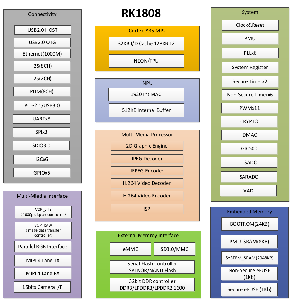
Rockchip RK1808 is the first chip from the company fully dedicated to artificial intelligence applications. The Neural Processing Unit (NPU) features an accelerator delivering up to 3.0 TOPS and is coupled with two low power Arm Cortex-A35 cores allowing it to run Linux.
We’ve had the specifications for RK1808 for a while, but the company has recently posted hardware and software resources on their open source website.
 On the hardware side we’ve got:
- RK1808 Technical Reference Manual (TRM)
- RK1808 datasheet
- PDF Schematics for the company’s official RK1808-EVB
On the software side we can get the Linux SDK from Github as explained in the Wiki:
|
1 2 3 4 5 |
git clone https://github.com/rockchip-linux/repo mkdir linux cd linux ../repo/repo init --repo-url=https://github.com/rockchip-linux/repo -u https://github.com/rockchip-linux/manifests -b master -m rk1808_linux_release.xml ../repo/repo sync |
Finally configure the build and start the build process:
|
1 2 3 |
sudo apt install liblz4-tool build-essential source envsetup.sh rockchip_rk1808 ./build.sh |
After a while, or more accurately close to two hours on a Laptop with Ryzen 7 2700U processor, 8GB RAM, and hard drive, we’ll get U-boot, Linux, buildroot based rootfs, and firmware files and in IMAGE/RK1808-EVB-V10_20190430.1810_RELEASE_TEST/ directory:
|
1 2 3 4 5 6 |
ls IMAGE/RK1808-EVB-V10_20190430.1810_RELEASE_TEST/ build_cmd_info IMAGES manifest_20190430.1810.xml PATCHES ls IMAGE/RK1808-EVB-V10_20190430.1810_RELEASE_TEST/IMAGES/ boot.img oem.img rootfs.img update.img MiniLoaderAll.bin parameter.txt trust.img userdata.img misc.img recovery.img uboot.img |
Now the only available development board is the RK1808-EVB from Rockchip which won’t be for sale to the general maker community, so we may have to patiently wait until one of the SBC’s companies decides to design one.
Thanks to Jon for the tip.

Jean-Luc started CNX Software in 2010 as a part-time endeavor, before quitting his job as a software engineering manager, and starting to write daily news, and reviews full time later in 2011.
Support CNX Software! Donate via cryptocurrencies, become a Patron on Patreon, or purchase goods on Amazon or Aliexpress. We also use affiliate links in articles to earn commissions if you make a purchase after clicking on those links.

The block diagram implies, and the RK1808 Datasheet confirms (page 31), that PCIe and USB3 are muxed on the same pins.
Yes, that’s the biggest fashion in tech in 2018/2019.
And a stupid thing to do imho.
While I do agree from a technical perspective (and a user’s perspective), these devices have a limited memory bandwidth and vendors probably don’t find it relevant to enable all high speed interfaces at once, and they consider that PCIe is almost never used on lwo-end devices. They probably figure that their device will either be a tablet or an STB, and that for the remaining 1% use cases needing both USB3 and PCIe (NAS) it is still possible to connect a USB3 controller to a PCIe bridge. This approach is definitely flawed and they’d rather not include PCIe at all if it’s to do that. They tend to see their chips as reconfigurable but once soldered to a PCB with connectors hanging at the end of the traces, it’s much less reconfigurable. One should also seriously wonder whether the PCIe IP in such SoCs has *ever* been tested, which is quite unlikely given the target audience.
So in short let’s simply consider such chips with mixed PCIe/USB3 have no PCIe, we’ll save time.
Isn’t the purpose of these shared interfaces to build USB3 connectors that implement ALT pin assignments for Apple Lightning?
Lightning isn’t even USB 3.0, it’s only 2.0. And no, it’s not for Thunderbolt either.
The muxed interfaces allow for lower pin-count parts, which lowers cost. However, if you want to say add proper WiFi over PCIe, then you lose out on USB 3.0. So it’s indeed a stupid implementation, especially moving forward, as 802.11ax seems to rely on PCIe rather than SDIO or USB as the preferred interface.
USB 3.1 supports PCI Express as an Alt-mode
https://www.anandtech.com/show/9331/intel-announces-thunderbolt-3
Anandtech is talking about Thunderboilt 3 being implemented as an USB-C alternate mode. And I wonder whether Synopsys or someone else provides a combined PCIe/USB3 IP block we see in more than one SoC appearing now…
No, it can not, Thunderbolt is the only interface for that, but the two more use the same connectors, but not the same cables.
Maybe the internal link between the RK3399 and the RK1808 inside the RK3399PRO uses this PCI connection?
It’s a combo phy (USB3/ PCIE) which can only operate in either USB3 or PCIE.
If you have a burning need for the RK1808-EVB it is for sale on taobao for $538. Two places have it listed.
https://item.taobao.com/item.htm?spm=a230r.1.14.1.57062d17A4C4UB&id=590286443304&ns=1&abbucket=12#detail
I suspect these two companies bought the kit to make their own PCBs and now are reselling the used kit.
I’m going to wait for a more reasonably priced board that includes a camera option. I know of five companies considering making a dev board for the RK1808 but so far no one has shipped one.
This is chip is for making embedded devices, it is not a good chip for running desktop Linux or building a NAS. But if you want to make a smart speaker or camera with AI, this chip is for you.
The only real flaw I see is that the h.264 encoder is underpowered. The chip supports 4K image sensors but the h.264 encoder only supports 1080P30. That really should have been 1080P60. If it was 1080P60 it could also do 4kP15 which is good enough. Come on, the ancient $3 Allwinner V3 supports 1080P60, seems like a brand new chip should support it.
The rumored Allwinner V5 successor with CNN support can do 4Kp30. Support for 4KP30 is a real winner.
I’m actually very interested in Cams where you leverage the NN as a cam that does networked camera function but does image recog at the camera, so you don’t need something beefy like NVidia’s offering.
In case anyone was wondering the NPU is Vivante VIP8000 not Ceva NeuPro as previously reported…
more precisely, Nano-Q: https://www.khronos.org/assets/uploads/developers/library/2017-embedded-vision-summit/13_VeriSilicon-Vision-Processor-Highlight_May17.pdf