
ASUS surprised the maker community in 2017 with the introduction of the Rochchip RK3288 powered Tinker Board to compete as Raspberry Pi 3 Model B. It was followed by Tinker Board S with built-in storage and other new features, as well as Tinker Board Edge T and Edge R SBC’s both with an AI accelerator namely Google Edge TPU and the NPU inside Rockchip RK3399Pro.
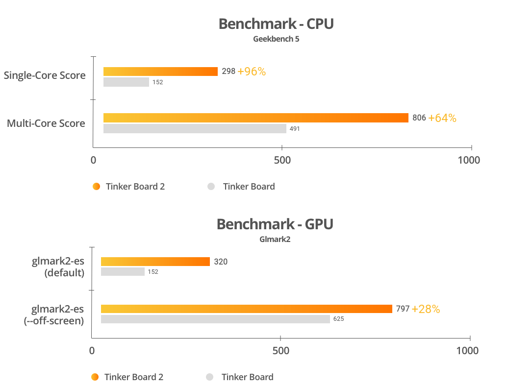
The company has now launched a new model called Tinker Board 2 without AI accelerator, but featuring Rockchip RK3399, or more exactly the higher grade Rockchip OP1 used in Chromebooks, delivering 96% faster single-thread performance and a 64% boost in multi-core performance compared to the Rockchip RK3288 processor found in the original Tinker Board, while the GPU is around 28% faster with glmark2-es2 off-screen benchmark.
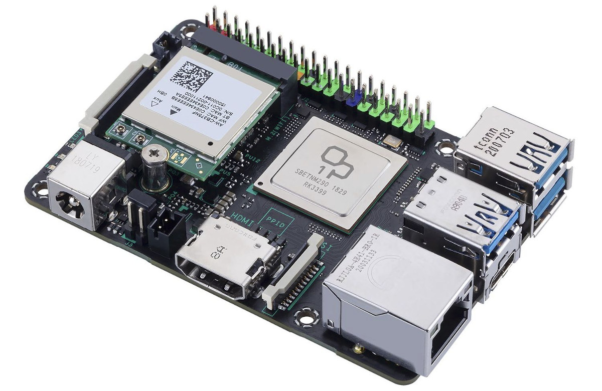
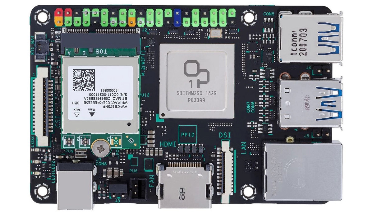
There are two variants of the board with Tinker Board 2 and Tinker Board 2S with the latter adding onboard eMMC flash storage. Both share the following specifications with bold highlights showing differences against the original Tinker Board:
- SoC – Rockchip 3399 (OP1) hexa-core processor with 2x Arm Cortex-A72 cores up to 2.0 GHz, four Cortex-A53 cores @ up to 1.5 GHz, Mali-T860 MP4 GPU @ 800 MHz
- System Memory – 2GB or 4GB LPDDR4, dual-channel
- Storage
- MicroSD slot
- Tinker Board 2S only – 16GB eMMC flash
- Video output & Display I/F
- 1x HDMI 2.0 up to 4Kp60 with HDMI CEC
- 1x 22-pin 4-lane MIPI DSI connector
- 1x DisplayPort 1.2 via USB-C port
- Audio –
1x 3.5mm audio jack;Realtek HD codec with 192KHz/24-bit audio
- Camera – 15-pin MIPI CSI connector
- Connectivity – Gigabit Ethernet, dual-band 802.11 b/g/n/ac WiFi 5 2T2R, Bluetooth 5.0
- USB – 3x USB 3.2 Gen1 host ports, 1x USB 3.2 Gen 1 Type-C OTG port
- Expansion Headers
- 40-pin header with GPIOs, SPI, I2C, UART, PWM,
2-pin contact point with 1x PWM signal, 1x S/PDIF signal
- Misc – Button, fan header, RTC battery header, power-on/recovery headers
- Power Supply – 12V to 19V via DC jack
- Dimensions – 85.6 x 54 cm
Besides the faster processor, the new Tinker Board 2 also supports more memory up to 4GB LPDDR4, adds a USB-C port with DisplayPort Alt mode, USB 3.2 ports, a faster WiFi 5 & Bluetooth 5.0 card instead of a soldered WiFI 4 + Bt 4.x module, and support for RTC.
The company will provide support for Android 10 (in Q1 2021) with support for the Android Neural Networks API 1.2 and Adiantum encryption, and “Pro-grade admin” tools such as the Asus IoT Cloud Console for data management and analysis, and “ASUS Industrial Android FOTA” for seamless upgrades of the firmware. Somehow there’s no word about Linux, albeit the original Tinker Board both Android and the Debian-based TinkerOS. Eventually, more details about OS support should surface on the documentation page.
 We still do not know when Tinker Board 2/2S will come out, and at what prices, but considering Android 10 is expected in Q1 2021, the launch should come soon enough. Additional information may be available on the products page.
Via Clubic and Liliputing

Jean-Luc started CNX Software in 2010 as a part-time endeavor, before quitting his job as a software engineering manager, and starting to write daily news, and reviews full time later in 2011.
Support CNX Software! Donate via cryptocurrencies, become a Patron on Patreon, or purchase goods on Amazon or Aliexpress. We also use affiliate links in articles to earn commissions if you make a purchase after clicking on those links.


Does the board support the WiFi AP (access point) mode?
Not sure yet. “AzureWave AW-CB375NF” is the model number of the M.2 card used on the board. It’s based on a RealTek RTL8822CE-CG chip.
Here’s the datasheet: http://www.azurewave.com/img/nvidia/AW-CB375NF_DS_B2_A_STD.pdf
Essentially, we’d need to figure out if the chipset supports, in AP mode, with vanilla Linux drivers, 802.11h DFS at 5 GHz. Unlike, say, the Intel chipsets.
Looks easy replace-able ? Good job Asus.
No m.2 sata/nvme I guess. Any shot of the board bottom side ?
P.S, USB-C > DC round jack. Bad job here Asus.
I could not find any photos on the bottom side.
> No m.2 sata/nvme I guess
No SATA of course but in case you find an adapter from Key A to Key M and are fine with Gen2 x2 speeds and a cable between board/adapter and SSD nothing will stop you from using NVMe. 😉
I think that is also no audio jack on this new tinker.
RK3399 is ready to be the king for some time now.
RK3588 or bust. I understand that RK3399 is well supported though.
yes, but it will be way more expensive and use vahalla, so no panfrost.. so noo good for me.
I really love the design of this board!
1) SoC on top – Its challenging to use anything with a bottom mounted heat-sink in a project. I can put this in a “normal” case.
2) Rugged barrel connector for power – USB-C does not provide enough current to drive all the USB ports on the board without an expensive “smart” adapter.
3) USB-C providing DP-ALT mode – there is no reason to have a USB-C connector if its only a USB3 port. The use of a stacked USB-A/USB-C connector is very clean.
4) M2 connector – While it currently has a wifi/bt board, I dream of replacing it with a 2-port SATA board. I hope ASUS makes the wifi/bt optional.
After containing my initial excitement, I am sure I will love everything about this board except for the price.
Same feelings here. I hope it doesn’t get as expensive as Vim3 Pro SBC from Khadas. Ex.Vim3Pro with essential accessories such as 24W USB-C Adapter, USB-C Cable, Case, heatpad for metal plate, New M2X Extension and shipping costs, it can easily reach $208 USD without including importing custom fees from your country(Usually around 30%).
Woah.. $208. When the asking price is this steep, I’ll resort to used laptop.
#3: I expect RPi (and others) to adopt this stack of 3x USB 3.0 Type-A, 1x USB Type-C within a revision or two. And DisplayPort Alt Mode over the Type-C port is ideal, although maybe more of them should be added to replace any Micro-HDMI ports.
#4: Even if they don’t, you can just unscrew and remove that?
The problem with the SoC on top in this design is that there are only 24x24mm available for a heat sink, i.e. nothing. So the board will constantly be throttling, unless you build a special case for it, which will be very expensive if you can’t benefit from the mass selling that RPi knows.
> 3x USB 3.2 Gen1 host ports
…should better read: 3 USB3 receptacles behind an USB3 hub of unknown quality sharing a single SuperSpeed (5Gbps) uplink to the SoC.
Is anything known whether USB2 data lines are populated on the M.2 Key A slot?
If you lookup the datasheet on the wifi/bt card in the picture, it states its PCIe(wifi)+USB(bt). This implies, but doesn’t confirm, USB is supported.
How does the RK3399 OP1 compare in performance to a S922X ?
For compiling and building tasks, S922X is much faster because has 4xA73 cores @2.4Ghz whereas RK3399 only 2xA72 ones. Ex.Building an exactly same image from eMMC module, it takes about 1.5hours on N2+ @2.4Ghz/2.0Ghz and 4 hours on RK3399 @2.0Ghz/1.5Ghz.
For I/O operations, RK3399 hands down specially when use along NVMe drive(1.3Gb/s average transfer speeds with Samsung EVO 970 plus m.2 drive)
> Building an exactly same image from eMMC module, it takes about 1.5hours on N2+ @2.4Ghz/2.0Ghz and 4 hours on RK3399 @2.0Ghz/1.5Ghz
This is strange even taking into account the slight clockspeed increase from 1.8 GHz to 2.4 GHz on the ODROID N2+, see Willy’s measurements: http://wiki.ant-computing.com/Choosing_a_processor_for_a_build_farm#Odroid-N2_-_2019-02-22
And asides ‘build farm’ workloads / use cases the CPU performance difference between RK3399 and S922X is even lower.
Willy’s also doing a very simple little build that only takes seconds to complete. That’s not very good for a benchmark. For example, it won’t show thermal problems, will it? For sustained use, the N2/N2+ HS/HSF setup will be hard to beat. Since they put the SoC on the wrong side of the board for decent cooling, this new Tinkerboard 2 will be hard to cool.
> this new Tinkerboard 2 will be hard to cool
On the plus side they use the more efficient OP1 RK3399 variant (those that reach higher clock speeds at lower voltages so generated heat will be lower compared to stock RK3399).
And of course S922X will be faster than RK3399 as long as the workload is not IO bound *. But not over twice as fast or only with very special workloads that are not representative for what majority of users will do with these things.
And you always just need to choose your benchmark wisely to proof whatever you want: https://browser.geekbench.com/v5/cpu/compare/4799810?baseline=3645019 😉
* with IO heavy workloads RK3399 with NVMe will beat every other SBC SoC around
It depends on the boards and how long they take to build. But the goal in these tests precisely is to know what can be reached with each board regardless of thermal issues, because when you want to assemble your build farm, you know you will have to deal with thermal issues anyway. Thus I want to pick the fastest possible hardware, then make it run without throttling (and pushing the thermal points to the maximum definitely is one of these factors :-)). But I agree that the N2+ is really interesting, it made me hesitate quite a bit. The H2 is even better for my use cases though.
At 2.4 GHz it could be up to 50% faster than the RK3399. It’s also possible that the RK3399 mentioned above started to throttle.
> At 2.4 GHz it could be up to 50% faster than the RK3399
Yes, an S922X clocked at this speed could be 50% faster but not more than twice as fast as has been reported above. It’s always the same:
Casual benchmarking: you benchmark A, but actually measure B, and conclude you’ve measured C.
Boring!!! RK3399 is old news.. Asus late to the party is all… We need something at least at 2.5 GHz now… Pi4 can run 2.2 GHz and Amlogic 922 is also above 2GHz it seems…
Just choose the ‘appropriate’ benchmarks and you’ll see that RK3399 outperforms S922X easily while RPi 4 is a close competition 😉
when Pi4 is running Android I will always doubt the benchmark… and are they OC or not?
> when Pi4 is running Android I will always doubt the benchmark
I would be concerned about totally different things when someone throws Geekbench numbers at me. 😉
Regardless of the OS in question Geekbench runs a bunch of (some more, some less) irrelevant CPU microbenchmarks and doesn’t monitor the environment it is running in.
This is comparing two times the exact same hardware (the ARM laptop I’m typing this on): https://browser.geekbench.com/v5/cpu/compare/4943670?baseline=4943571
Looks like the M1 or MacOS is intelligent one, with caching. Could you try again, but with different scenario: test1, then do something else about 2 hours, then, test2.
> Looks like the M1 or MacOS is intelligent one, with caching
The M1 SoC is impressive [1] and macOS tries to make the best out of it.
The ‘problem’ here is that Geekbench behaves as crappy as every other kitchen-sink benchmark available since it doesn’t stop when background activity is too high. I simply fired up another benchmark in parallel to ruin the 2nd testing but Geekbench did not stop to mark the results invalid (which is easy to spot especially since Geekbench shortly pauses between the individual benchmarks).
Geekbench scores are questionable in general but this behavior of uploading whatever invalid results have been collected makes the tool worthless for performance comparisons. But since it’s aimed at clueless people who love to stare at graphs representing numbers without meaning nothing will change here.
[1] Still setting up a monitoring environment to explore performance/watt and energy savings behavior: https://github.com/ThomasKaiser/Knowledge/blob/master/articles/Exploring_Apple_Silicon_on_MacBookAir10.md#cpu-performance-assessment
rk3399 is old news?? it’s a 28 nm SoC, the same as the “new” RPI4 one, but it have 2-3 times more powerful GPU and TONS of I/O compared to rpi4. overall is way better than RPI4.
CPU speed is just a feature. first, all the engineers at RPI don’t recommend clocks higher than 2.0 bc it severely compromise lifespan. second, your “desktop usage” limitations are GPU on that crappy broadcom SBC, not CPU.
Their performance numbers are totally exagerated. I suspect they’ve looked for the benchmark that emphasized the interest of their new device. For me, RK3399 gives roughly the same performance as RK3288. If you have few threads/processes, RK3288 is faster thanks to its 4 powerful cores vs only 2 on the RK3399. If you have plenty of tasks to run, some will run slower on the RK3399 but you’ll complete 50% more in the same time. I found that the RK3399 is easier to cool than the 3288.
With this said, the board is an overall improvement and it’s nice that they’ve dropped the nasty 5V input!
12V min input is pretty high. I wish it were 7.5V or similar like the newer HK boards support:N2, H2, C4.
I’m cheap and lazy, so I wish they went up to 20V or just above so I can use recycled 19V-20V laptop power bricks. But 12V is easy to get in bulk as well with used server power supplies. For when you have to feed a lot of boards.
Oh, I want to add one other thing. I really love boards that don’t use a 5V input. Why? Because it means they’re using a regulator (likely switching because linear regulators with 19V input that supply even one 500mA USB port will cook a hole through a board). The benefit of that is they will have current limiting on their outputs! They’re not going to have a piece of copper on the PCB go directly from the input to the output in such a way that a shorted output can cause the PCB to catch fire. Having done that in the past, I really appreciate boards that aren’t vulnerable to it!
This memory was triggered by my previous comment about using used server 12V supplies to feed boards. When you have a 50A 12V supply, you want to limit current to your loads! A little SBC does not need 50A. If it should try to draw it and you let it, very bad things start to happen.
Remember, any wire is a fuse if you put enough current through it.
HI, I think 5v type C with PD (soz higher voltage if you want) should be a must for an ARM SBC. 5V gibe you the flexibility to power it just farting harder than usually
No, 5V is terrible because everything that needs 5V will get less due to the small losses accumulating over the long power cable and the connector. It’s very common to see 4.4-4.6V on the 5V pin of various boards under load. Some USB devices automatically disconnect then. Some USB3 external hard drivers spend their time spinning up and down on boards powered on 5V. The *only* reason vendors made this mistake of using 5V as the power input is that it allowed these boards to be powered from a regular USB port. The rule is simple: you should never use the same voltage for input as what you’re supposed to deliver on output (unless of course you’re employing a buck-boost regulator on board).
A power cable must always be placed before a regulator. For example I have a USB-to-12V cable that I’m using to power my Clearfog directly from my laptop. I’m pretty sure that the USB port falls to 4.5 or so under load but I don’t care as long as it’s turned to 12V and back to the appropriate voltages on the board.
not having 5V option (remeber, option) harm flexibility. on rockpi4 I can use 5V, 9v ..even 19v
I agree with you, I’d have preferred 7-to-20V but 12-19 is better than 5 alone. Regarding the fact that each wire is a fuse, it’s true unless you use micro-USB to power the board, as the cable and the connector’s resistance usually spread their share of power so that the board gives up at the end of the chain. Usually you’ll at least have P-channel MOSFETs to deliver the juice to the USB ports, and these ones will turn off when the voltage is too low anyway. But I’ve already seen a few explode as well 🙂
So why not just install a inline fuse on the cable near the power end, safer and cheaper than burning wire or sbc.?
I argue that you should have a fuse per board. Fuses can be used to protect sources, loads, and distribution. A fuse at the source protects it from too much load (good power supplies have this built in as a protection circuit). A fuse at the source end of a wire protects the wire from a short along its length. A fuse at the load protects the load from drawing too much current. Fuse all the things!
Or, built other methods of current limiting into sources and loads. USB does this (or is *supposed to*) by monitoring current draw and limiting it. Some have no control over their loads, some use (as Willy mentions) just a P channel MOSFET to at least be able to turn on and off a load. But a good one will have a load controller that acts as a programmable fuse and also reports current draw.
but why not 5V with the option to use up to 19v IF YOU WANT.. like on Rockpi 4C
As an *option* yes. And indeed, 5->19 is an exceptionally wide range.
The reason you’re unlikely to see a 5 volt and up input like that is because the regulator will have to be a buck/boost type instead of the much simpler and more common buck. Since you have to be able to generate 5V from this input, you have to accept less than that as an input (unless you’re saying it can fail if the voltage drops below 5V exactly which mean no powering it from USB which is what I think you want 5V compatability for) and boost that up to 5V, but if it’s >5V, you have to drop that down.
Chips to do this are available, but they’re less common, more expensive, less efficient, and require more complicated support parts (MOSFETs, etc.).
I think at this point we just should be thankful that we have something better than a crappy micro-USB jack for power. Asking them to include even more complex and expensive power input circuitry may be going too far.
I rather have NVMe or PCIe with NVMe hat than USB 3.2.
I also don’t trust ASUS supporting their own board and the community. They know they can have a quick buck without doing much here.
The Tinker Board is a joke. It was dated when it was released. And the only SBC that ever died on me, without using it much. I was so stupid to buy a 2nd without using it. I’m not wasting my money again on their board.
Their motherboards are was better products.