
Nobody likes to change or recharge batteries in their IoT nodes, so any new development related to energy harvesting or batteryless devices is welcomed. Renesas RE01B is a new Bluetooth 5.0 Low Energy (BLE) Arm Cortex-M0+ MCU that consumes at little as 35 µA/MHz during operation and 600 nA during standby making it suitable for battery maintenance-free IoT devices, or even batteryless IoT devices thanks to its energy harvesting controller.
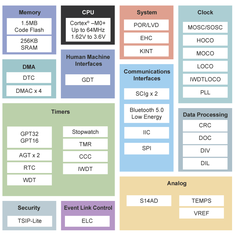 Renesas RE01B microcontroller’s features and specifications:
- CPU – Arm Cortex-M0+ core up to 64MHz
- GPU – 2D graphics accelerator
- Memory – 256KB SRAM
- Storage – 1.5MB flash
- Connectivity – 2.4 GHz radio with Bluetooth 5.0 Low Energy; up to 400m range (Long Range) and 2 Mbps data rate
- I/Os
- 8x PWM outputs
- 7x 14-bit A/D converters (ADC, Analog inputs)
- SCI (UART), I2C, SPI
- Timers
- 1x 32-bit Timer, 3x 16-bit Timer, 2x 8-bit Timer
- 2x Watchdog Timer, 1-second event timer, stopwatch
- Oscillators – Low-speed 32.768kHz, middle-speed 2MHz, high-speed 64 MHz
- Security – TSIP-Lite (Trusted Secure IP Lite)
- Misc – PLL, RTC, Power-On Reset, Low Voltage Detection, Energy Harvesting Controller
- Supply Voltage – 1.62V to 3.6V
- Power Consumption
- 35 µA/MHz (using internal LDO) or 15 µA/MHz (using ISL9123 DC/DC converter) during operation
- 600 nA (core: 500 nA, Bluetooth: 100 nA) during standby
- Peak current of 3.0 mA (1Mbps) during Bluetooth reception and 4.3 mA during transmission (0 dBm, 1Mbps)
- Package – 64-pin QFN (8×8 mm)
The company explains the “on-chip energy harvesting control circuit (rapid startup capacitor charging and secondary battery charge protection functionality) allows users to achieve battery-less Bluetooth communication” and that “energy harvesting and power storage can be directly connected to the RE01B”.
Renesas APIs includes various profiles such as Heart Rate Profile (HRP), Environment Sensing Profile (ESP), and Automation I/O Profile (AIOP), in addition to the Bluetooth 5.0 protocol stack, and support for over-the-air (OTA) firmware updating

Development tools for the RE Family include QE for BLE program which generates custom Bluetooth profiles that can be integrated into the user’s own application programs, and a Bluetooth Test Tool Suite GUI to perform initial wireless characteristics evaluations and Bluetooth functionality verification.
Tessera Technology also developed the EB-RE01B evaluation board to get started with the new chip features including energy harvesting, and reference designs for a low-power wearable and a GNSS tracking device are in the works.
Renesas RE01B is available now, and EB-RE01RB can apparently be purchased now (price no public) with shipment scheduled for the end of April. More information and the wireless MCU can be found on Renesas website, while you may want to check out Tessera’s product page for further details about the EB-RE01B evaluation kit.

Jean-Luc started CNX Software in 2010 as a part-time endeavor, before quitting his job as a software engineering manager, and starting to write daily news, and reviews full time later in 2011.
Support CNX Software! Donate via cryptocurrencies, become a Patron on Patreon, or purchase goods on Amazon or Aliexpress. We also use affiliate links in articles to earn commissions if you make a purchase after clicking on those links.

Where is it harvesting the energy from?
Some undefined “power generating device” that needs to be connected to the board.
After skimming through the datasheet: The term “energy harvesting controller” seems slightly misleading. The chip supports slow supply voltage ramp-up and safely charging a storage element, while being powered from another source. This makes it easier to integrate the chip with harvesting solutions like a DC/DC boost converter. While you may be able to directly connect it to a harvester, like a solar panel, this would require good matching of the operating points and will most likely be inefficient.
Attached is the diagram of their “energy harvesting controller” from page 284 of the device user manual. If the chip was basically this unit coupled with plain basic Cortex-M0+ or RV32E with some GPIO produced inexpensively it would have been a wonderful chip. This chip they produced, however, is a solution looking for a problem.