
The SGET (Standardization Group for Embedded Technologies) non-profit organization ratified another system-on-module standard last November, with the “Open Standard Module” (OSM) standard that instead of relying on edge or board-to-board connectors is meant to be soldered on the carrier board as a solder-on module LGA package.
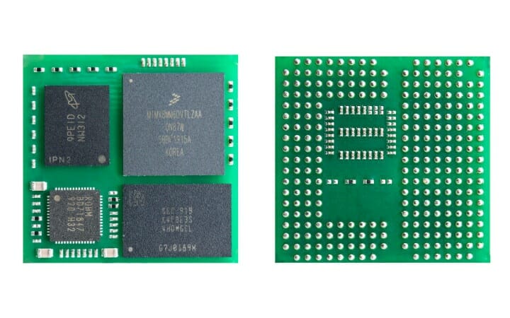
F&S Elektronik has unveiled one of the first SGET OSM compliant SoM with “FS 8MM OSM-SF” equipped with an NXP i.MX 8M Mini processor, up to 8GB DDR4, 32GB eMMC flash or 512MB NAND flash on a 30x30mm “Size-S OSM” form factor.
FS 8MM OSM-SF system-on-module
 FS 8MM OSM-SF module specifications:
- SoC – NXP i.MX 8M Mini single, dual, or quad-core Arm Cortex-53 processor @ 1.8 GHz with real-time Cortex-M4 core @ 400 MHz, Vivante 2D & 3D GPU, 1080p60 H.265, VP9, H.264, VP8 video decoder
- System Memory – Up to 8GB LPDDR4
- Storage – Up to max. 512MB SLC NAND flash or up to 32GB eMMC flash
- 332 balls contact grid with
- Storage – 2x SD card interfaces
- Display
- 1x 4-lane MIPI DSI interface
- Analog resistive and PCAP Touch ext. via I2C
- Camera I/F – MIPI CSI interface
- Networking – Ggiabit Ethernet
- USB – 1x host, 1x OTG 2.0
- Serial – 1x CAN, 4x UART
- 4x I2C, 2x SPI, up to 32 digital I/Os, PWM
- Audio – I2S, ESAI, SAI, SSI, SPDIF
- RTC
- Supply Voltage – 5V DC/±5%
- Power Consumption – 3W typ.
- Dimensions – 30x30mm (Size-S “Small” OSM)
- Weight – 7 grams
- Temperature Range – 0°C – +70°C; optional: opt. -20°C – +85°C
The company provides supports for Buildroot & Yocto to build a custom Linux image running on the Cortex-A53 core(s) and FreeRTOS for the Cortex-M4 microcontroller. The module will be available until 2029.
Open Standard Module (OSM)
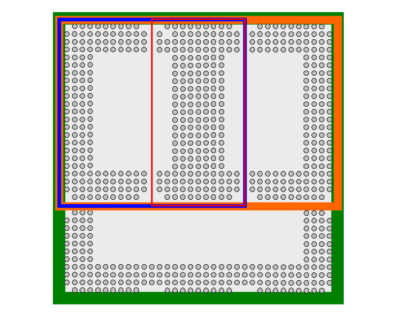
While F&S Elektronik currently only announced a”Size-S” OSM module, there are four different sizes defined in the specification.
- Size-0 – “Zero”: 30 mm x 15 mm with 188 contacts (see red outlines above)
- Size-S – “Small”: 30 mm x 30 mm with 332 contacts (see blue outlines)
- Size-M – “Medium”: 30 mm x 45 mm with 476 contacts (see orange outlines)
- Size-L – “Large”: 45 mm x 45 mm with 662 contacts (see green outlines)
The document also details all pins with only a few being mandatory (e.g. UART, RTC), and most being simply recommended or optional.
While I believe it’s the first industry-wide system-on-module standard that is meant to be soldered, some companies introduced their own private standard in the past with for example TechNexion XORE, and we’ve seen many application processor modules with castellated holes or pads.
Only limited details are available on F&S Elektronik’s product page at this time, but the company will host a webinar on May 6th with plans to discuss the advantages and challenges of using a solder-on-module following the OSM standard, and how to start development.

Jean-Luc started CNX Software in 2010 as a part-time endeavor, before quitting his job as a software engineering manager, and starting to write daily news, and reviews full time later in 2011.
Support CNX Software! Donate via cryptocurrencies, become a Patron on Patreon, or purchase goods on Amazon or Aliexpress. We also use affiliate links in articles to earn commissions if you make a purchase after clicking on those links.

This is odd idea, as people use SOMs to escape from the BGA routing and PCB soldering complexity.
So what is the point to put BGA ICs on BGA carrier PCB? and place some filtering capacitors around the balls 🙂
The point being pin-to-pin compatibility when (re)designing products. I think this is a great idea and I hope there will be enough support to make it an industry standard.
Btb-connector does not suit automative, agricultural, large machinery, etc as there is usually too much vibration.
I believe it’s like products of Octavo Systems – packaging away complexity of DDR routing and density that comes with these pins (i.MX 8M Mini has 486 pins, I’m pretty sure remaining 154 pins are almost completely used to connect to these 3 ICs on module). I see 2 potential advantages to this approach:
I believe any PCB design with 1.25mm BGA ball pitch is much easier than 0.65mm/0.5mm raw BGA devices. I think I can make a square hole to make a room for the bypass capacitors on the SOM.
Anyway, I also prefer traditional B2B or SODIMM connectors for easier soldering and debugging if my carrier board is big enough to mount a bigger SOM.
I agree with Tsvetan.
I would prefer a castellated solution with concentric pinouts for different sizes (each module use only the outer), with fewer pins using only serial interfaces: I2C, SPI, I2S, USB, CSI, DSI, CAN, including the ethernet PHY to reduce pinout, etc.