
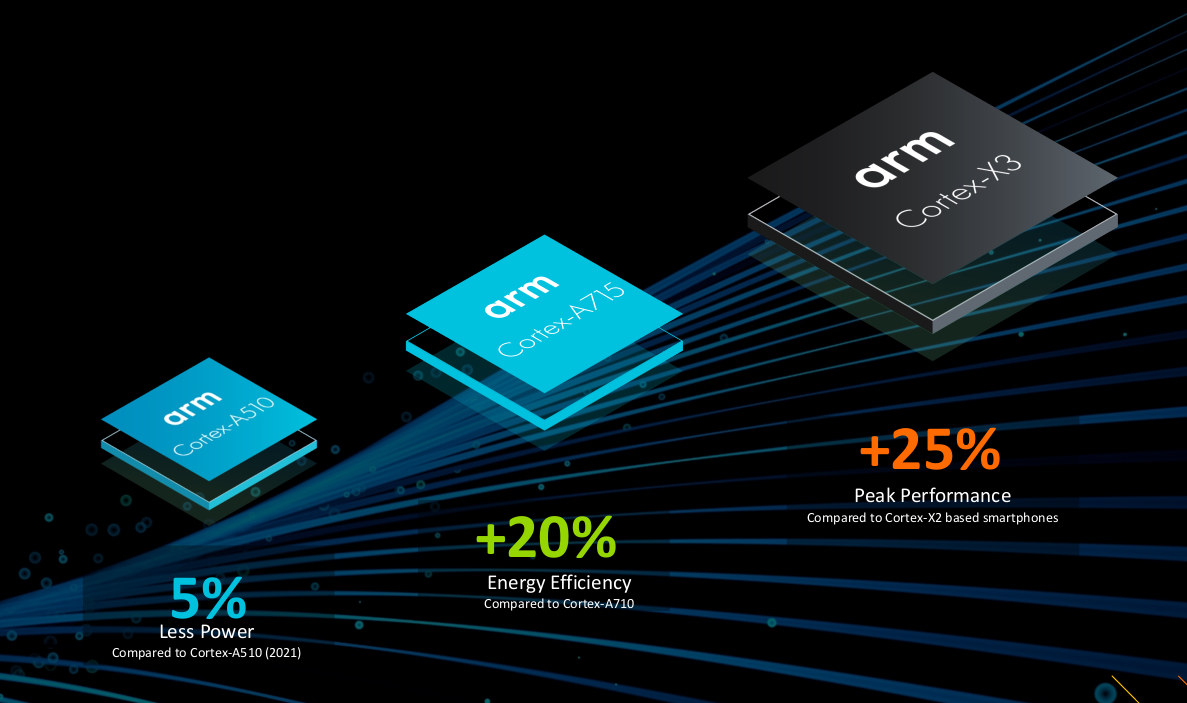
Besides announcing the new Immortalis-G715, Mali-G715, and Mali-G615 GPUs, Arm has also introduced the second-generation of Armv9 cores with the Cortex-A715 and Cortex-X3 cores with respectively a 20% energy-efficiency improvement (and smaller 5% performance uplift) over the Cortex-A710 core and a 25% peak performance boost against the Cortex-X2 flagship core.
The announcement also includes a “refresh” of the Cortex-A510 core announced last year with a 5% improvement in efficiency and the same level of performance. The Cortex-X3 will also be used in (Windows 11) laptop processors with the single-thread performance improved by up to 34% in that case.
Armv9 mobile SoC (Total Compute) in 2023
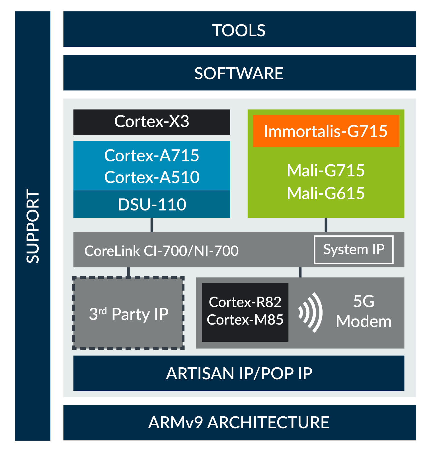 Future Armv9 flagship mobile SoC worked on this year, and released in 2023 should have a combination of Cortex-X3, Cortex-A715, and Cortex-A510 cores, an Immortalis-G715 GPU, a new DSU-110 “DynamIQ Shared Unit” that supports 50% more cores in CPU clusters (or up to 12 cores per clusters) with up to 16MB L3 cache, and a 5G modem equipped with Cortex-R82 and/or Cortex-M85 cores.
Arm expects up to 28% more performance and up to 16% power reduction across a range of workloads, such as gaming, to enable longer play time. Processors will be offered with up to 8x Cortex-X3 CPU cores and 4 Cortex-A715 CPU cores for premium laptops delivering up to 120% performance improvement in GeekBench 5 compared to existing (2021) Arm-based laptops with 1x Cortex-X2, 3x Cortex-A710, 4x Cortex-A510. Another interesting tidbit is that the Cortex-A715 now matches the performance of the Cortex-X1 announced in 2020.
More technical details may be found in a post on Arm’s community website.
Arm CPU & GPU roadmap to 2024
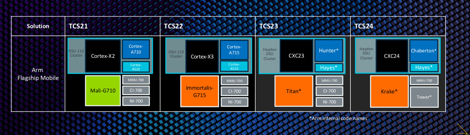
Arm also divulged a simplified roadmap for 2023 and 2024 designs with new cores codenamed Hunter, Chaberton, and Hayes (LITTLE core), a new Hayden DSU (for even larger clusters?), and a new interconnect codenamed “Tower” appearing in the 2024 IP. The new GPUs for 2023 and 2024 also have their own codenames, respectively Titan and Krake. There aren’t any public details, but at least we’ll roughly know that those are if they appear in silicon vendor roadmaps.

Jean-Luc started CNX Software in 2010 as a part-time endeavor, before quitting his job as a software engineering manager, and starting to write daily news, and reviews full time later in 2011.
Support CNX Software! Donate via cryptocurrencies, become a Patron on Patreon, or purchase goods on Amazon or Aliexpress. We also use affiliate links in articles to earn commissions if you make a purchase after clicking on those links.


And here we are, still waiting for an SoC with Cortex-A76 to become available in the realm of the SBC.
That’s indeed a big difference between ARM and x86, but it also stems from the fact that they don’t build chips but sell IP. In the x86 world you have both IP and the chip, and in addition instead of being SoCs they focus hard on pinout compatibility. The result is that in the ARM world when a new core is launched, it takes 3 years before it sees a customer, while in the x86 world it can take a few weeks/months.
> when a new core is launched, it takes 3 years before it sees a customer
Since talking about A76… core announced May 2018 and Huawei Mate 20 based on HiSilicon Kirin 980 available Oct the same year. So with a highend SoC for flagship phones few months seem possible.
I would believe ‘the realm of the SBC’ is also defined by SoCs originating from the ‘Android e-waste’ world where everything takes a lot more time.
Probably but it will take as long (or even longer) to see a laptop compared to an SBC… The reason being as usual that everything needs to be ported, there’s no way to perform a drop-in replacement of a CPU with another on an existing PCB with its voltage regulators, memory, boot parameters etc.
>The result is that in the ARM world when a new core is launched,
>it takes 3 years before it sees a customer,
And you have 2 customers minimum: ARM finishes the design and releases it, then some fabless SoC vendor has to integrate into their template of interconnected half working IP blocks and get some engineering samples made up. Then someone that’s going to put that chip into something has to decide the chip is worth using, design something around it and order enough parts for the SoC vendor to actually start producing parts. If all goes well after a year or more of hacking up the Android code to make it all functional a product might be released to consumers.
>while in the x86 world it can take a few weeks/months.
I’m not sure how it is for AMD as they don’t have their own fabs but I can imagine that Intel can have engineering samples for new CPUs and the support chips in the hands of integrators a lot quicker than anyone else.
x86_64 {workstations(?), desktop, laptop}mainboards were designed (3-5yrs) in advance of e.g. tpm upgrade modules (Win10->Win11 (1.2)2.0 “(soft)hard requirement” considering security updates, server&office&production environments)
even rpi’s (Pi 4, Pi 3B+, Pi 3, Pi 2, Pi 1, Pi Zero, Pi 400 <- SPI (extension cable) ) include tpm compatibility
(thx, no tpm on ARM devices in general)
x86_64’s know volatile markets and customers?
The note about the “power efficient” A715 now reaching the performance of the not-so-old X1 is very interesting. This means that they’re really focused on increasing performance and have noticed that it’s what has been missing the most for a long time, and that the market is ready to adopt more powerful chips. On one of their slides it’s mentioned that the perf numbers are for an X3 at 3.3 GHz in the smartphone comparison, and at 3.6 GHz in the laptop comparison. They’re definitely getting closer to competition in the mid-range. Long gone are the days where you would only have four A53 as efficiency cores to help the poor two A72, and I think it’s a good thing.
Bring on the fast 12-cores. It seems nobody was going to bother with dual-cluster in consumer devices (for 16 cores) so here we are.
Apple’s M cores slow down in progress considering performance/efficiency compared to that huge advantage on M1 introduction.
Several difficulties on tiny node sizes and increasing cost/technical_improvement vs. additional declining ressources (?), but for all {x}pu high-tech companies (and somewhat saturated markets, now)
Just for the clarification:
Total Compute: high-end platform
Total Solution: IoT platform
So, I recommend changing ‘Total Compute Solution’ to ‘Total Compute’
thanks
I’ve changed it, but in the presentations given to the press, one of the slides reads:
You are right Jean-Luc. Probably, ‘Total compute Solutions’ is the commercial name.
IoT platforms will end up being “Total Solution solutions” 🙂 That’s a bit awkward…
Arm needs more markets and Smartphone/Cellphone market is saturated. Arm keep looking at Server market, while RISC -V nibbles at Arms toe nails.
Competition is good 😁
Seems confusing. Should have renamed it A511. A whole extra digit is right there.
If it’s the same core why should the name change? Since chip designers estimated ‘up to 5% more efficiency in some special cases’ that turned into ‘a 5% improvement in efficiency’ when marketing department wrote the announcement?
This is the stuff that matters to distinguish between different cores and if the relevant bits haven’t changed incrementing numbers for marketing purposes just confuses and wastes people’s time.
Sometimes it depends. If you remember RK3288 that was announced as Cortex A12, then the A12 definition improved over iterations as they were likely the only A12 customer, to the point where they started to advertise it as A17, with a paper covering it and writing “A12”, till finally ARM said that A12 and A17 were the same and that A12 was dead. The only leftover probably was the model ID on the RK3288 that still said A12 while being in (almost) all points equivalent to an A17 🙂
> The only leftover probably was the model ID on the RK3288 that still said A12
It’s really 0xc0d pointing to A12 while MT6595’s A17 cores show the correct ID 0xc0e.
If it’s not a new core, can launched/announced products with Cortex-A510 get the same efficiency boost?
Efficiency alone is hard to measure because it will change with a different process node and different voltage. So the same way as the A53 evolved between different process nodes and may be found between 40 and 10nm, there will be significant power efficiencies for a same core in different contexts.
All roads lead back to ARM making confusing announcements for the sake of marketing.
To be fair with them, it’s not for the sake of marketing but because they’re selling IP and not silicon. The difference is huge. They’re just providing you with a schematics saying “if you assemble the transistors this way you’ll get the documented behavior for this model”, and it’s almost only your problem to choose the exact transistors model. In the x86 world, vendors give model names to the silicon chip itself, thus it implies everything. If ARM didn’t change the behavior at all and possibly only slightly rearranged a few points resulting in better power usage, it’s just a revision of the same model and it’s reasonable not to give it a new name. After all, I’m having A72rev1 on my mcbin and A72rev3 on other boards, and they probably have more differences (i.e. bugfixes) than just a slightly lower consumption.
> launched/announced products with Cortex-A510 … efficiency boost
Huh? Which ‘products’ and which ‘boost’? The ‘5%’ are marketing BS just like majority of the rest of this ‘announcement’. The numbers are guesses at best or simply just BS. Who measured energy consumption of existing A510 SoCs from 2021 and 2022? Nobody since not existing.
Check this slide here. Read the percentages and their meaning below: ‘Projected Geekbench 5 MT scores, thermally unconstrained‘. BS numbers by design (Geekbench total scores) combined with gazing in a crystal ball.
But this marketing strategy always works since technical journalists copy&paste the percentage ‘values’ as if they were real measurements or the thruth instead of a marketing department’s guesses and/or obscure simulations.
Power consumption of A510 cores have been measured by chinese youtuber geekerwan, from the d9000 and 8 gen 1.
You are referring to this, right: https://youtu.be/cAOwLW2jXuQ?t=130
If so where/how has this guy measured the consumption of a ‘core’ especially a little one?
No, this one https://youtu.be/kkrzM7i64oE?t=850
At around 14:10 mark.
Check few seconds before: https://youtu.be/kkrzM7i64oE?t=832 – he’s not comparing ‘cores’ but different nodes and different fabs. And while the process names sound similar they’re just marketing BS as well: TSMC’s 5N process is not 5 nm and 4N is not 4nm and whatever Samsung does with its process names has also zero relationship with chip/transistor structures.
And unfortunately his methodology is severely flawed since he is only able to measure the consumption of a whole device to then do some ‘math’ to substract this and that to come up with some (polished) numbers to back whatever claims a Youtuber needs to make (remember: his target audience are relatively dumb people not able or willing to read any more).
But who cares? Nobody. Since people love to trust blindly into any numbers thrown at them if they’re just presented nicely. Superiour graphical representation always helps in fooling people. Though people who are still able to read avoid YT for a reason… and on the other hand Google navigates consumers to all this crappy YT content also for a reason.
Asides that this seems to be one of the less than ten ‘YT IT channels’ that do not totally suck 🙂
Yeah, the measurements might not be accurate, but i dont think anyone else even did anything. Probably the best you can find.
Even if we know they’re truly a marketing company (just looking at the scale-less graphs with growing curves is enough), it’s pretty possible to accurately estimate power draw from the structural models without having real silicon. This is needed anyway to avoid hot spots on the chip. Of course we know that “up to 5% savings” basically means “we found a single unexpected case where the peak consumption was 4.58% lower than on the previous version”, but it really *is* possible and normal to estimate such measures just like it’s normal to be able to refine some data paths to save a bit of power by reworking some parts that previously had to be released in an inglorious state. Minor reworks of some very hot paths around the register file or L1 cache can have significant impacts on power usage at high frequencies.
> it’s pretty possible to accurately estimate power draw from the structural models without having real silicon
Sure. And this has happened. The 1st slide of ARM’s announcement shows for the new A510 ‘Up to 5% power reduction’ so this is the maximum under ideal conditions and the expected result of ongoing development resulting in slight improvements here and there.
But not an ‘efficiency boost’ and especially nothing that could be measured by comparing real silicon made in different fabs on different nodes.
> But not an ‘efficiency boost’ and especially nothing that could be measured by comparing real silicon made in different fabs on different nodes.
Of course, not a “boost” at all, only an improvement. And yes it can vary a lot between fabs, and even between successive waffers of a same fab. That’s also why they may only speak for the part that’s within their responsibility: providing a better design that should slightly improve consumption when all other conditions remain equal. That’s not bad in any case and always good to have. But it’s indeed not a “boost”.
I think this is a bigger improvement than expected, but maybe still need to take some caution with those numbers.
I’m most excited to see the return of EL0-aarch32 mode in Cortex-A510v2. Even if this is the last core we’ll see supporting that mode, it will make a nice replacement for Cortex-A53/A55 in memory constrained embedded systems. It should now also be possible to have an A710+A510v2 system with aarch32 user space capable of running on all cores rather than the ugly hack that was added for A510v1.
What did the hack consist in before this ?
https://www.kernel.org/doc/html/latest/arm64/asymmetric-32bit.html
Ah yes, I remember now about these CPUs which do not support the same instruction sets between different clusters of the same SoC! I didn’t know that some work had been going on there. Interesting, I’ll read it deeper, thank you Arnd!