With the Star64 and VisionFive 2 single board computers, we’ve already got two hardware platforms based on the StarFive JH7110 quad-core RISC-V processor, but somehow we did not get the detailed specifications of the new processor, and some details such as the presence of AI accelerators or exact PCIe specifications were lacking.
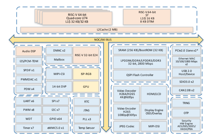
Some documentation for the StarFive JH7110 processor has been released and answers some of those questions. It’s actually an SoC with six RISC-V cores, of which four 64-bit RISC-V cores run the main OS, plus a 64-bit RISC-V monitoring core, and a 32-bit RISC-V real-time core. The AI accelerators found in the JH7100 (Neural Network Engine and NVDLA) appear to be gone for good, and there are two 1-lane PCIe 2.0 interfaces up to 5 Gbps each.
StarFive JH7110 specifications:
- CPU sub-system
- Quad-core 64-bit RISC-V SiFive U74 (RV64GC) processor @ up to 1.5 GHz with 32KB D-Cache, 32KB I-cache
- Single-core 64-bit RISC-V SiFive S7 (RV64IMAC) monitor core with 16KB I-cache, 8KB DTIM
- Single-core 32-bit RISC-V SiFive E24 (RV32IMFC) real-time control core with 16KB I-cache
- Up to 2MB L2 cache
- GPU – Imagination BXE-4-32 GPU with support for OpenCL 1.2, OpenGL ES 3.2, Vulkan 1.2
- Video Decoder – H.265, H.264 4K @ 60fps or 1080p @ 30fps, MJPEG
- Video Encoder – H.265/HEVC Encoder, 1080p @ 30fps
- Memory
- BUS RAM up to 256KB
- Up to 8GB DDR4/3, LPDDR4/3 at 2133/2800 Mbps
- Storage
- 2x SDIO/eMMC 5.0 host controllers
- QSPI controller for up to 16MB SPI flash, up to 2GB SPI NAND flash
- Display interfaces
- 1x HDMI 2.0 up to 4Kp30
- RGB656, RGB888 up to 1080p30
- MIPI DSI up to 2.5 Gbps or 1080p30
- 1x DPI (Parallel RGB Display)
- Camera interfaces
- 1x MIPI CSI-2 interface up to 6 lanes of 1.5 Gbps; support for 1x 4D1C or 2x 2D1C MIPI sensors up to 4Kp30
- 1x DVP sensor input interface
- Audio
- 32-bit audio DSP used for traditional audio/voice data algorithm processing
- 8-channel TX and RX I2S/PCM TDM
- 4x sets of I2S/PCM I/F with DMA support
- 2x sets of SPDIF I/F, RX and TX modes
- 4-channel PDM input for digital MIC
- DAC output with PWM interface
- Networking – 2x Gigabit Ethernet with RMII/RGMII
- USB – USB 3.0 host/device (multiple with one PCIe interface), USB 2.0 host/device
- PCIe – 2x PCIe 2.0 x1 up to 5 Gbps per lane (Note one of the PCIe 2.0 interface is multiplexed with USB 3.0)
- Other peripherals
- 6x UART, 7x I2C, 7x SPI
- 2x CAN 2.0B Bus up to 1 Mbps
- 7x 32-bit timers, 1x 32-bit WDT reset output
- 1x temperature sensor
- 3x GPCLK outputs
- 2x INTC
- 8x PWM outputs
- 64x GPIO
- Security
- Encryption: AES; DES/3DES; HASH; PKA
- Compliant with TRNG
- 256-bit random number generation
- 512 x 32-bit (2 KB) of OTP for key data on-die storage
- Clock sources
- 24 MHz for USB, GMAC, and system main clock source
- 32.768 kHz for RTC clock source
- Voltages
- 0.9V core voltage
- 1.8V/2.5V/3.3V I/O voltage
- Boot modes
- Boot Rom
- QSPI NOR/NAND Flash
- SD card/eMMC
- UART/USB/SD card update
- Package – 17 x 17 mm, 0.65 mm ball pitch, FCBGA package with 625 balls
Supported operating systems include Linux, VxWorks, and other RTOS.
Target applications for the StarFive JH7110 processor include single board computers, home NAS, routers with software routing, Smart Home appliances, industrial robots, drones, and video surveillance applications. The documentation website comes with a product brief and a datasheet, and a hardware design reference plus a software developer guide are also in the works.

Jean-Luc started CNX Software in 2010 as a part-time endeavor, before quitting his job as a software engineering manager, and starting to write daily news, and reviews full time later in 2011.
Support CNX Software! Donate via cryptocurrencies, become a Patron on Patreon, or purchase goods on Amazon or Aliexpress


That’s a lot of great features on one SoC. Nice.
So what stopped them going with PCIe 3x ?
maybe they (yet) don’t provide the internal necessary bandwidth for system bus ((Bus Matrix), (off-chip: RapidIO,) on-chip: TileLink, ARM AMBA, etc.?) for all configurations of ‘CPU sub-system’ and with all (peripherals) concurring raw data/protocols (, cost for IP?)
Absolutely. We tend to forget about the internal bus sizes and cache bandwidths, but not so long ago a reputable vendor (NXP) managed to fail their iMX6 with GbE being limited to 470 Mbps just due to internal busses. Now we’re speaking about speeds that are 20 times larger and this requires careful handling.
> managed to fail their iMX6 with GbE being limited to 470 Mbps just due to internal busses
More some other design flaw. More than a decade old i.MX6 featured also a single Gen2 PCIe lane (though lacking DMA support) and some cluster guys measured +350 MB/s which translates to 2800 Mbit/sec or 3500 Mbit/sec whether you want to apply 8b10 coding or not.
[ some fuzzy assumptions for a consumer market device SoC (what depends a lot on SoC production volume, starting from scratch, but having general experience on design process) for a tablet, smart phone, set-top box or game console like device and on established, current node sizes (selecting target clock rate conservatively was recommended)
NRE: ~$20,000,000
• $5M NRE to Silicon Integrator (eSilicon, GUC, etc.)
• $5M for IP
• $2M for CAD tools
• $8M for engineering salaries and expenses
IP: ~$5M (licenses)
• $0.5M CPU core
• $0.5M Memory Controller
(• $0.8M NOC)
• $2.5M external Interconnect (SERDES)
• $0.5M on-chip SRAM
• $0.2M other IO interfaces
• $0.8M PCIe Controller (excl. SERDES, ~3.0)
if it’s a low volume (~1k) development task, having no priority on area, but being critical on design schedule/risk and performance at power, NRE could/would be roughly ~92% of overall cost, while fabrication NRE %7 (~$1.5M) and production 1% (~$215/pc.) [DARPA research, ~2015].
(and no firmware/software cost (possible variety!) added) ]
Well things are getting crazy, the other company SiFive has agreed to sell OpenFive, including their custom SoC IP to Alphawave IP. The design smarts need and IP for good SoC are out there.
seen with system bus documentations, there’s a ~50% share for commercialized licensing for Risc-V cores, while the other half is open sourced for distribution w/o licensing cost for the cores
some, Risc-V cores often combined with ARM system environment (AMBA -> [bus] AHB, APB, [interface (bus, protocol)] AXI …..) with ARM providing “the software ecosystem, comprising development tools, operating systems, drivers, and applications guaranteed to run on compatible CPUs.” (including experience from billion devices)
or
combined with custom system environment from scratch (e.g. OpenCore’s (Silicore) Wishbone bus, IBM CoreConnect)
How much of “free” SoCs (with Risc-V, being free cores) are free from (IP) licensing cost?
github.com/riscvarchive/riscv-cores-list
e.g. RV32IM instructions, test SoC github.com/ultraembedded/riscv_soc
at the moment Risc-V shows faster progress, support for community (dev) tools, specialized hw accelerators inclusion and tendency for ~lower consumer prices compared to ARM (being more advanced, on e.g. X3, A715, G715 and maybe NPUs?, but also more standardized) (?)
[ for above ~1k dev example: cost (incl. NRE, market startup) for each pc. ~$21.750, for ~1M sample production cost (incl. NRE) is reduced to ~$29 ]
Intel seem RISC V keen.
” New Intel Pathfinder for RISC-V platform enables developers to create their own products using RISC-V cores and IP from the partner ecosystem, instantiate on FPGA and simulator platforms, and run operating systems and tool chains within a unified IDE. “
embedded.com
JH7110?
If this chip’s components could all be used from one RTOS, that woild be amazing for my use cases.
forget arm!
Not that simple, more complex a multi level market.
RISC V needs to embrace open source GPU drivers and open source I/o peripheral drivers. Having to write new USB, HDMI, Sata etc drivers for every new SoC needs to end. That’s how you reduce costs and reduce e waste. IMHO
Designs seem to embrace off the shelf Vivante and PowerVR; I am not sure how these 2 don’t meet your categorization of “open source GPU drivers” since they both have Mesa contributions – in PowerVR’s case I would encourage them to continue along the path despite cynicism in the past week on this forum.
If you were expecting some sort of Larabee/Cell RiscV-specific GPU solution, I’m afraid that went awry when Libre-SOC chose OpenPOWER.
Actually part of what to expect was known for about a year. JH7110 was originally planned to be a heart of BeagleV, before they started to redesign it from scratch. And because of that overall ideas (amount of cores, frequency, what GPU, amount of PCIe lanes) were public since approx. March 2021.
The removal of the neural processing blocks is really not a big deal, because the two PCIe 2 lanes allow the user to pop in a Coral TPU* (which has a way better software ecosystem than most SoC specific NPUs). I think it was a smart move to focus on IO rather than a flashy NPU block.
Tangentially, I was a little disappointed to see that the video encoder/decoder blocks only support MPEG-LA codecs (no VP8/9 or AV1 support). Oh well those are not even going to be used for all use cases. I wonder if the CPU can decode VP9 at high resolutions! Maybe.
Is it known which process node / fab was used? I’m really interested in a benchmark comparison with the rk356x, but it would be nice to set expectations 😉
* https://coral.ai/products/m2-accelerator-ae
StarFive have posted a preliminary technical reference manual.
It’s technically something, but specifically useless (hopefully only for now).
Oh man am I disappointed.