
Last year, Andes introduced the AndesCore 27-Series of Linux capable RISC-V cores with a vector processing unit for AI acceleration with specifically the 32-bit A27 and the 64-bit AX27 cores. The company also introduced the higher-end AndesCore 45-series (A45 and AX45) at about the same time, but we somehow missed the announcement.
Andes has now added more Linux capable RISC-V AndesCore to the aforementioned families with the high-performance superscalar A45MP and AX45MP multi-core processors, and A27L2 and AX27L2 processors with an L2 cache controller.
Andes A27L2 and AX27L2 cores
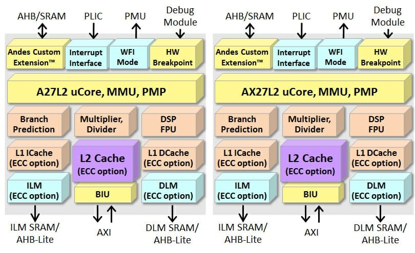
Based on the highlights, the new cores look identical to the A27 and AX27L2 cores announced last year expect the additional L2 cache that comes with optional ECC.
AndesCores A27L2 and AX27L2 key features and specifications:
- AX27L2 – 64-bit, 5-stage pipeline CPU architecture (RV64GCPN), enabling software to utilize the memory spaces far beyond 4GB
- A27L2 – 32-bit, 5-stage pipeline CPU architecture (RV32GCPN)
- AndeStar V5 Instruction Set Architecture (ISA), compliant with RISC-V technology
- Floating-point extensions
- DSP/SIMD ISA to boost the performance of voice, audio, image, and signal processing
- Andes extensions, architected for performance and functionality enhancements
- Separately licensable Andes Custom Extension (ACE) for customized
- acceleration
- 16/32-bit mixable instruction format for compacting code density
- Branch prediction to speed up control code
- Return Address Stack (RAS) to speed up procedure returns
- Memory Management Unit (MMU), Physical Memory Protection (PMP) and
- Programmable Physical Memory Attributes (PMA)
- Level-1 and level-2 cache controllers with 64-byte cache line size
- MemBoost for heavy memory transactions
- Flexibly configurable Platform-Level Interrupt Controller (PLIC) for supporting a wide range of system event scenarios
- Enhancement of vectored interrupt handling for real-time performance
- Advanced CoDense technology to further reduce code size on top of “C” extension
The L2 cache enables the doubling of memory bandwidth and reduces memory latency by 70%.
Andes A45MP and AX45MP multi-core RISC-V processors
Andes has not added product pages for the new multi-core A45MP and AX45MP cores, but based on the information known from the earlier A45 and AX45 and the press release, A45MP and AX45MP cores should have the following key features:
- AX45MP – 64-bit in-order dual-issue 8-stage pipeline CPU architecture (RV64GCPN) supporting clusters of up to 4 cores
- A45MP – 32-bit in-order dual-issue 8-stage pipeline CPU architecture (RV32GCPN) supporting clusters of up to 4 cores
- AndeStar V5 Instruction Set Architecture (ISA), compliant with RISC-V technology
- DSP/SIMD extensions
- Floating-point extensions
- Andes extensions, architected for performance and functionality enhancements
- 16/32-bit mixable instruction format for compacting code density
- Advanced low power branch predication to speed up control code
- Return Address Stack (RAS) to accelerate procedure returns
- Memory Management Unit (MMU), Physical Memory Protection(PMP), and programmable Physical Memory Attribute (PMA)
- Optional L2 cache controller
- MemBoost for heavy memory transactions
- Flexibly configurable Platform-Level Interrupt Controller (PLIC) for supporting a wide range of system event scenarios
- Enhancement of vectored interrupt handling for real-time performance
- Advanced CoDense technology to reduce program code size
That means the new A45MP and AX45MP cores get support for multi-core and an optional L2 cache, and are expected to be used in SoC found in ” heavy-duty” applications such as AR/VR, AI/machine learning, 5G, In-Vehicle Infotainment (IVI), Advanced Driver Assistance Systems (ADAS), video/image processing, enterprise-grade storage device, and networking.
You’ll find more details on Andes’ AndesCore processors page. Right now, only A27L2 and AX27L2 pages are up, but the company should soon add more details about the new multi-core 45-series cores.
Via LinuxGizmos

Jean-Luc started CNX Software in 2010 as a part-time endeavor, before quitting his job as a software engineering manager, and starting to write daily news, and reviews full time later in 2011.
Support CNX Software! Donate via cryptocurrencies, become a Patron on Patreon, or purchase goods on Amazon or Aliexpress. We also use affiliate links in articles to earn commissions if you make a purchase after clicking on those links.


These and micro magic will finally see high GHz RISC v SoC, hopefully.
I’ve seen that Micro magic news a few days ago, but I skipped. The photo is odd. They show the 0.69 mA after CoreMark benchmarks. Maybe that RISC-V core does not implement DVFS an always runs at 3+ GHz. Also as I understand it, Micro magic is not an IP company, they provide EDA tools to designs IC, so that core will likely never be manufactured.
Which would be a real shame if it was genuine and able of such speed.
This is from a post I made over at the HardKernel forums where this test chip was being discussed:
“they provide EDA tools to designs IC, so that core will likely never be manufactured.” Exactly. A showcase of their tools.
Furthermore, the person who did / announced it, is a freelancer / contractor, AFAIK
The problem is that if you search for “order”, there is no “out-of”. It’s all “in”. 2 issue is good. but no register re-writing. slow. If you want to win, 4 issue. 6 issue. 8 issue. out of order. I mean, honestly, let’s give arm (and apple, and samsung and qualcomm) a run for their money. This is isn’t rocket science.