
Allwinner D1s (aka F133) is a cost-down version of Allwinner D1 RISC-V processor introduced earlier this year together with a Linux capable development board, with the main difference being the integrated 64MB DDR2.
Besides the built-in RAM, Allwinner D1s comes with many of the same features as D1 RISC-V SoC, but loses HDMI output and the HiFi 4 audio DSP, and Allwinner made some tweaks to the IOs with one less I2S audio interface, and general-purpose ADC.
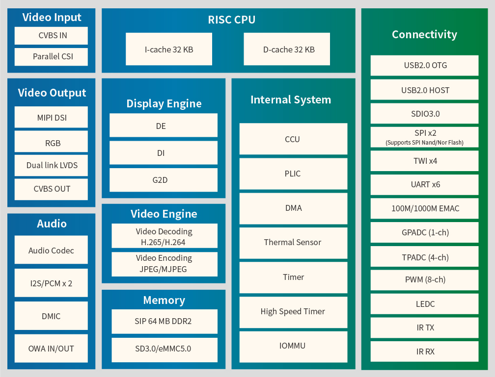
Allwinner D1s/F133 specifications:
- CPU – RISC core with 32 KB I-cache + 32 KB D-cache (CNXSoft: not specified, but probably the same Alibaba/T-Head Xuantie C906 RISC-V core as used in Allwinner D1)
DSP – HiFi4 DSP 600MHz with 32 KB I-cache + 32 KB D-cache, 64 KB I-ram + 64 KB D-ram- Memory – 64 MB DDR2 (SIP)
- Storage I/F – SD3.0, eMMC 5.0, SPI Nor/Nand Flash
- Video Engine
- Video decoding
- H.265 up to 1080p @ 60fps
, or 4K @ 30fps - H.264 up to 1080p @ 60fps
, or 4K @ 24fps - MPEG-1/2/4, JPEG, VC1 up to 1080p @ 60fps
- H.265 up to 1080p @ 60fps
- Video encoding – JPEG/MJPEG up to 1080p @ 60fps
- Supports input picture scaler up/down
- Video decoding
- Video OUT
- RGB LCD output interface up to 1920 x 1080 @ 60fps
- Dual-link LVDS interface up to 1920 x 1080 @ 60fps
- 4-lane MIPI DSI interface up to 1920 x 1080 @ 60fps (Note: shown in block diagram, but not in the specs)
HDMI V1.4 output interface up to 4K@30fps- CVBS OUT interface, supporting NTSC and PAL format
- Video IN
- 8-bit parallel CSI interface
- CVBS IN interface, supporting NTSC and PAL format (only for F133-B processor)
- Display Engine – Allwinner SmartColor 2.0 post-processing engine, de-interlace support, G2D hardware accelerator
- Audio
- 2x DAC’s and 3x ADC’s
- Analog audio interfaces – MICIN3P/N, LINEINL/R, FMINL/R, HPOUTL/R
- Digital audio interfaces – I2S/PCM, DMIC, OWA IN/OUT
- Networking – 10/100/1000M EMAC with RMII and RGMII interfaces
- USB – USB2.0 OTG, USB2.0 Host
- Other peripherals
- SDIO 3.0, SPI x 2, UART x 6, TWI x 4
- PWM (8-ch), GPADC (1-ch),
LRADC (1-ch), TPADC (4-ch), IR TX & RX
- Security Subsystem
- AES, DES, 3DES encryption and decryption algorithms
- RSA signature verification algorithm
- MD5/SHA and HMAC tamper-proofing
- Hardware random number generator
- Integrated 2 Kbits OTP storage space
- Package – eQFPA 128 14×14 mm
- Manufacturing process – 22nm
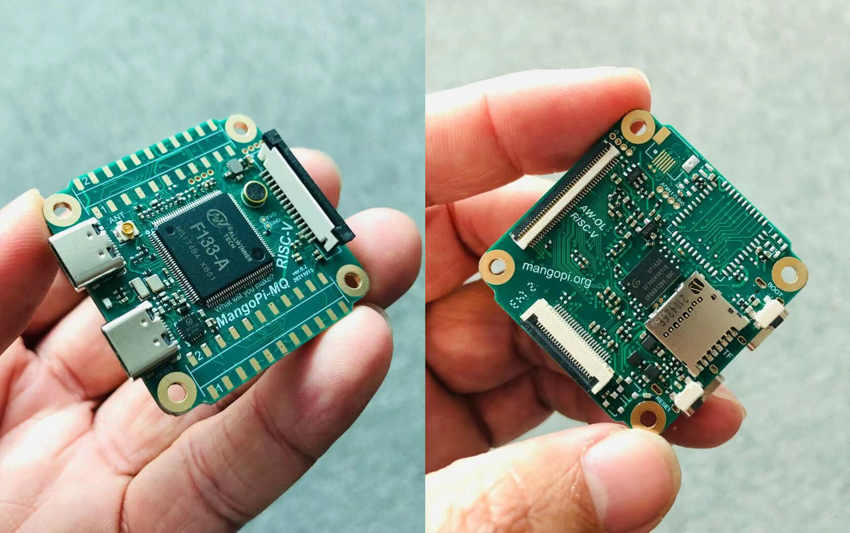
The processor page on Allwinner’s website does not mention RISC-V at all, only RISC, but I found about the processor via the MangoPi team who teased us with the upcoming MangoPi-MQ1 SBC based on Allwinner F133-A processor, so I can confirm it’s indeed a RISC-V processor.
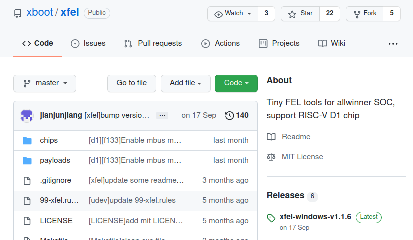
For further confirmation, the xfel FEL tool for Allwinner D1 on Github also supports F133. Supported operating systems include Melis RTOS based on RT-Thread, and Tina Linux (OpenWrt).
Allwinner D1s looks to be designed for cameras and smart displays and offers peripherals, embedded RAM just like Allwinner V3s or SigmaStar SSD210 Arm-based processors. Boards based on Allwinner D1s/F133 should be very cost-effective with Linux-capable RISC-V SBCs likely to sell for $10+ and up. We’ll know soon, as MangoPi-MQ1 mass production is scheduled for November, and the board should start selling on Taobao and Seeed Studio soon after.

Jean-Luc started CNX Software in 2010 as a part-time endeavor, before quitting his job as a software engineering manager, and starting to write daily news, and reviews full time later in 2011.
Support CNX Software! Donate via cryptocurrencies, become a Patron on Patreon, or purchase goods on Amazon or Aliexpress. We also use affiliate links in articles to earn commissions if you make a purchase after clicking on those links.


OK, nice … but with Linux on 64MB RAM … can you run python? gcc?
Or will it be an openwrt experience, with only small tools like wget and ls?
> but with Linux on 64MB RAM
…you might want to get rid of systemd and disable unneeded services as much as possible otherwise this will be a rough ride 😉
If you carefully cut down Systemd, it can run on a 486 w/ 20M memory (This is what is done on AOSC OS/Retro) 😉
Well I must admit for a ordinary Systemd installation 256M memory should be necessary…
I forgot to write about OS support, now updated. Allwinner lists Melis OS (RT-Thread RTOS), and Tina Linux (OpenWrt).
Is it only me or anyone else remembers Linux being run on 4MB RAM on 80368 machines?
“run”? Linux on 4MB took minutes to boot, and X was even slower. That was around 1995 or so.
That boot time was just because it waited for all the services to come up completely over the network, I believe. I wrote a revision to the FreeBSD colonel that launched all the services in parallel and it booted in 10 seconds which resulted in a visit to our company from Jordan Hubbard. (Freebsd sponsor).
Not quite. I think the earliest I used was a Pentium with 16 MB of RAM. FVWM was glorious.
I deployed an 1.6 MB Linux-based router booting on a floppy. Yes, 640kB + 1024 kB extended memory on a 386SX. The floppy was a hybrid format I used to create myself by then with 18 sectors/track for the kernel (so that the BIOS can load it), switching to 21 sectors/track for the rootfs. pppd and ipfwadm were running on it. That wasn’t fast, but it did work. By then (1994) my development machine had 8 MB and would run XFree pretty fine in 800×600. Of course gcc was used quite a lot. By then it was fast and light 🙂
When i first started using linux, then the smallest i know, Damn Small Linux, needed 32MB RAM (text mode).
Now, the smallest I use is Tiny Core needs 46 MB Ram to boot.
and my lowest ram “PC”, RPi 1 has 512mb ram.
4MB ram requirement must be pre 2.4 kernel.
i dont have internet connection at home back then lolz.
You’ll need to use busybox for most things but python3 and other stuff is very much doable.
> You’ll need to use busybox for most things
Not necessarily, my Breadbee’s rootfs uses standard coreutils, util-linux etc. With an XZ-compressed squashfs, there’s lots of room for a full-blown system, which doesn’t take more RAM than its size on the flash. Better, on low-memory systems, use an mtdblock and mount it directly from the NOR (though that’s usually quite slow).
Using standard core utils sounds good because sometimes busybox can be really annoying .. it’s tar always makes my head hurt 🙂
The vendor SDK for the 2 x cortex A7 chips with 64MB of DDR2 that are kicking about now drives a 1024 x 768 LCD with a nice colourful UI, has a hardware video decoder streaming video into the UI etc. If you can get away from thinking that Debian is a lightweight distro then these small systems are very capable and you can get them on a 2 layer board from JLCPCB.
Not surprised at all. Windows 95 recommended to have 8 MB of RAM on a PC to run Internet Explorer at this screen resolution. It just depends how much we’re willing to waste resources due to laziness, as usual.
Renesas RZ/A is full of A9 cores bound to even less than that, with top loadout being 10MB, yet it’s still promoted for HMI and similar applications.
If they’d kept the h.264 encoder this would have been a good replacement for the Allwinner V3/S3. Any pricing yet? I would guess under $3. One could hope for $2.
Does anyone know if they pinned out rgmii on F133? They didn’t on V3s.
I wonder if it will have same problems as D1/Nezha?
could you elucidate which problems …
since it’s so expensive, not many people got that board, and those who did blame memory controller for lackluster performance.
Man, this really blurs the line between microcontroller and “single board computer”. It loses almost all its RAM and HDMI vs the D1.
I guess it’s semantics, but I usually think whether you can run an OS that allows you (the human) to interact with the computer and change how applications run; vs a microcontroller that simply runs preloaded code when powered on.
And I guess it qualifies by that simplistic measure. But I wonder what would you do with this besides build a smart camera …?
The rule of thumb I use — if it has an exposed parallel bus it is a SOC, no exposed bus it is a microcontroller. This SOC has an exposed bus between the two dies inside the package. On microcontrollers you can’t get to the bus. Of course there are exceptions to this.
The differentiation between applications and microcontrollers is easier with Arm. Arm Cortex-M is typically found in microcontrollers, while Cortex-A cores are always found in application processors, although some Cortex-M7 parts (e.g. i.MX RT series) probably cross the line.
With other parts like ESP32 I’m often conflicted, some times I call it a microcontroller, other times a processor.
>some times I call it a microcontroller, other times a processor.
I don’t think anything produced recently is a processor. If you think about a processor like the mc68000 you get just a CPU core and some basic interrupt logic. Everything else like DRAM controller etc is external.
I think I prefer the fixed application vs OS + loaded applications criteria.
If you have a fixed lump of ROM where all of your code needs to be and a smaller amount of RAM then you have a microcontroller.
Things are a bit blurred when you have hardware that is microcontroller-like (No MMU etc, low frequency) but code in RAM and a few megabytes of RAM so you could in theory load applications in and out at run time.
Unless Allwinner changed something this SoC is both a generic computer (application grade RISC-V, mmu etc) and a microcontroller (Whatever they are using for the power management micro).
The ESP32 remains confusing there. For example you have a boot loader with a menu on the Odroid-GO that allows you to select the application you want to load. It’s definitely closer to the MCU, but well, having run CP/M under an emulator on it further blurs the distinction!
No exposed parallel bus, ESP32 is a microcontroller. PSRAM is a peripheral.
With this definition you can have microcontrollers with a lot of power. For example if you integrated flash and DRAM with an x86 core on a single die. But I don’t think that is buildable with current technology.
I understand but I was showing that it can be troubling to declare it a microcontroller while running a full-blown CP/M on it. And similarly the 8051 *is* a microcontroller and has multiple parallel busses. But these are corner cases, and regardless I’d still tend to agree with your definition.
Can you get to the parallel bus on an 8051? Every CPU has a bus, but on microcontrollers you can’t get to them because they are not brought out to pads on the die.
I don’t recall ever seeing an 8051 chip with as exposed address and data bus.
Not only it does, but it’s how you connect external RAM and ROM! And the ROM-less 8031/8032 only work with this. From my memory, there were 4 32-bit I/O ports, 2 or 3 of which could be assigned either to memory or to I/O. The bus looks a lot like the 8088’s in minimal mode, with multiplexed address and data, and with a pin indicating if the access is for program or data. I remember having soldered 28-pin DIL sockets on top of original RAM to support an EPROM allowing me to replace internal programs. That was fun 🙂
I think it can be seen as a reasonable rule nowadays. However 8051s would break that one.
I tend to use a different rule, considering that if your registers and/or I/Os are memory-mapped and directly accessible without MMU etc then it’s an MCU. Said differently, does the setup code for the LED blinking code outweight the loop or not 🙂
every Intel CPU (8080. 186. 286. 386) up to Pentium fails that test. There are many large CPUs without MMUs.
286 and 386 have MMUs. I/O can be reserved for the OS on these machines. Of course both boot in 8086 mode.
Zilog eZ80 has it’s internal bus exposed in I/O, just a sidenote.
I would not call the eZ80 a microcontroller. It is derived from the Z80 which is a full CPU.
How is the Z80 full CPU different to a Cortex M? really?
AFAIK Cortex-M does not bring the address and data bus to pads on the die where it can be accessed. That is my rule for telling the difference.
There’s no reason you couldn’t do that if you really wanted to.
You could get on ARMs Design start thing, get the CPU core IP for a Cortex M0, dump it in an FPGA design where the top level exposes the AHB or whatever interface the CPU uses out to pins.
I think if directly exposing the CPU interface is required to not be a microcontroller then almost everything is microcontroller now.
SoCs have brought processors much closer to microcontrollers than in the past, thanks to all the stuff integrated inside, so it’s true that it becomes hard to draw a line.
Regardless there’s still one that holds well: the input voltage range. MCUs usually accept wide ranges and sometimes support batteries without any regulator, while CPUs and SoCs have extremely tight ones requiring an external power controller.
>SoCs have brought processors much closer to microcontrollers
>than in the past, thanks to all the stuff integrated inside,
>so it’s true that it becomes hard to draw a line.
I’m not going to claim to be an expert here but even on current non-SoC X86 CPUs you don’t get external access to the CPUs native bus AFAIK.
You get the external part of the DRAM controller and something like DMI (for Intel) to connect to whatever chipset you have to drive PCIe slots etc. Maybe DMI is close enough to the CPU that it counts but it’s pretty far removed from getting a bunch of address bits, data bits and bus control that is driven directly by the CPU.
>SoCs have extremely tight ones requiring an
>external power controller.
But then there are SoCs like the imx6 that have integrated power management and LDOs so that they only need a core and io reference supply which is pretty close to MCUs. 😉
Someone has already made an opensource board:
https://hackaday.io/project/182389-the-cheapest-risc-v-64-computer-by-now
Chips seem to be on taobao too.
I can’t figure out magic phrase on taobao to show me the chips.
Found this..
https://whycan.com/t_6440.html
datasheet, SDK, schematics, etc
https://item.taobao.com/item.htm?spm=a230r.1.14.33.7a5053eeH5V1rd&id=656231775496&ns=1&abbucket=5#detail
$5.50? I wonder what the real price from Allwinner is?
Probably not $5.5 when the world gets back to normal.
The dual Cortex A7 chips don’t cost that much.
Is there a method to access that page without having to login/create an account?
Looks like you worked something out.
I thought taobao let you look at a few items before forcing a login. Maybe they always force login now? I can’t even remember how I created my account now .. 😀
MangoPi-MQ is completely open source. After the test is completed, the Kicad-based hardware project will be released to github