Lattice Avant is a new low-power and small form factor mid-range FPGA platform, manufactured with a 16nm FinFET process, and equipped with 25 Gb/s SERDES, hardened PCI Express, external memory PHY interfaces, a high DSP count, and a security engine.
Lattice Semi is better known for its entry-level FPGAs such as the iCE40 which is popular in the community thanks to low-cost hardware and support for open-source tools, but the Avant platform marks the company’s entry into the mid-range FPGA market, defined by chips with 100k to 500k logic cells (LCs).
Lattice Avant highlights:
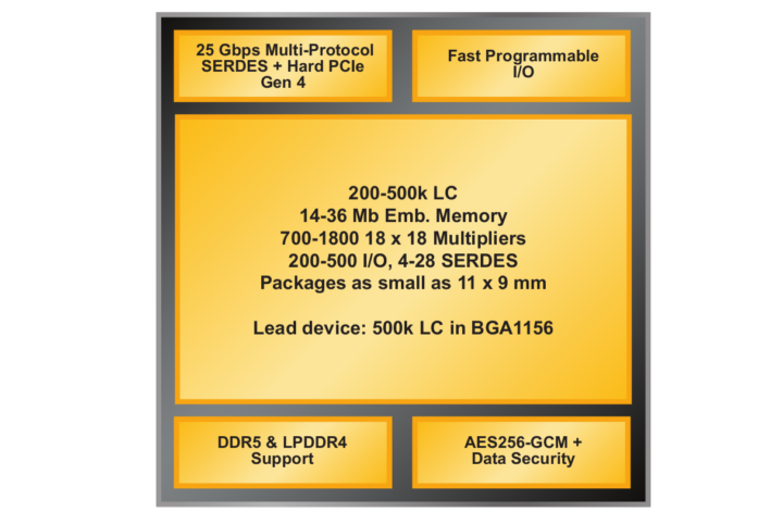
- FPGA fabric – 200K to 500K logic cells up to 350 MHz
- DSP – 700 to 1,8000 18×18 multipliers @ up to 650 MHz to support the latest AI algorithms
- Memory
- 14-36 Mbit embedded memory up to 650 MHz
- DDR3L/DDR4/LPDDR4 and DDR5 support
- I/Os
- 4x to 28x 25 Gbps multi-protocol SERDES
- Hard PCIe Gen4
- 200 to 500 I/Os
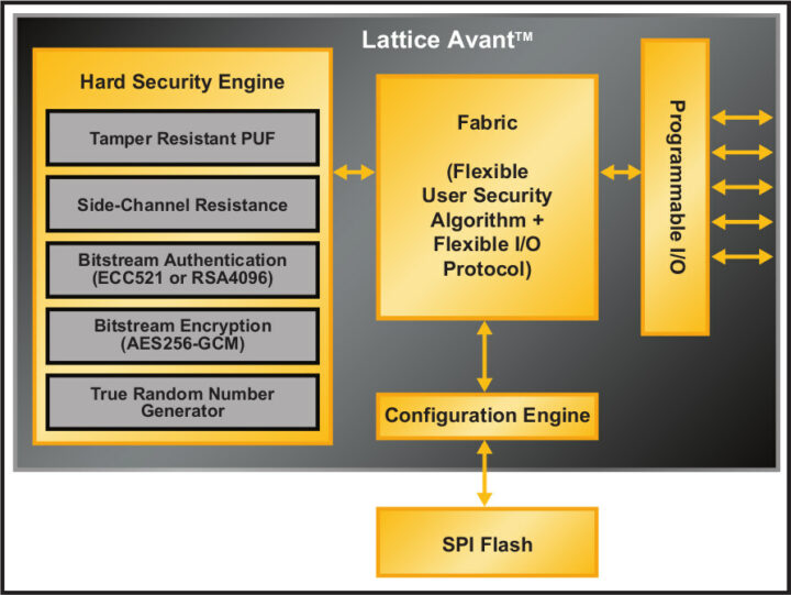
- Security engine with AES256-GCM encryption, ECC521 or RSA4096 authentication, tamper-resistant PUF, side-channel resistance, TRNG
- Lower power than similar class competitive devices thanks to a four-input LUT implementation, a reduction in high-capacitance nets, and the low-leakage 16nm process
- Package (Avant-E family)
- 11 x 9 mm for 200k LC
- 15 x 13 mm (BGA1156) for 500K LCs

Lattice Semi will provide the Lattice Radiant and Lattice Propel tools that include compiler optimizations and analysis to let users develop FPGA applications on the Avant FPGAs more easily. Lattice Avant is also said to come with a suite of IPs either hardened (custom logic) configurations for optimized area and performance, or in soft format (through the use of logic cells) for more flexibility.
The Avant FPGAs are expected to be used in networking controllers, PLCs, Edge computers, machine vision, industrial robotics, automotive networking and software-defined radio, as well as indoor 5G small cells and 5G fronthaul applications.
The company has a few demos with the Avant FPGA including a power consumption comparison against Intel Arria V and Xilinx Kintex-7 FPGAs, which shows the competing solutions consume 2.3 to 2.5 times more power. The Lattice Avant FPGA performance is also up to twice as fast as similar devices and comes with an up to six times smaller package. Lattice Semi claims this was made possible as competitors do not focus on the mid-range, using high-performance designs with a smaller logic cell count and less memory capacity, while they optimized the Avant FPGA specifically for mid-range use cases.
Besides just announcing the Avant platform, Lattice introduced the Avant-E FPGAs available in industrial and commercial grades with three SKUs: Avant-AT-200E, Avant-AT-300E, and Avant-AT-500E.
What’s unclear to me is when those FPGAs will be broadly available, as right now the company asks interested companies to contact their sales representative. More details may be found on the platform page, the Avant-E product page, and the press release.
Thanks to TLS for the tip.

Jean-Luc started CNX Software in 2010 as a part-time endeavor, before quitting his job as a software engineering manager, and starting to write daily news, and reviews full time later in 2011.
Support CNX Software! Donate via cryptocurrencies, become a Patron on Patreon, or purchase goods on Amazon or Aliexpress. We also use affiliate links in articles to earn commissions if you make a purchase after clicking on those links.


@Jean-Luc Aufranc
There’s a bizarre bug that’s making all the Underscore text also Strikethrough text.
Looking at the page source… it appears that there’s a WordPress plugin trying to validate the links and marking them all as broken by styling them with Strikethrough. Maybe your host machine’s DNS resolver is broken. Or maybe Lattice’s host is blocking your host’s IP range.
Apologies. That’s the broken link checker plugin I’m using that’s not playing nice with the Lattice Semi website. It should be OK now.
Very interesting. Always nice to see more serious players in this FPGA space. It doesn’t look like these will support open source tools any time soon though.
They have not learned from the toolchain around ice40.
Help? I don’t get the comment? I have worked with smaller lattice models and actually found the tools ok. Is issues related to bigger models or general? And compared to altera/intel or xilinx?
A huge driver of ice40 series popularity in more amateur space is the very well made open source toolchain available. Most really big customers would’ve probably picked it anyways, since it’s honestly the best “tiny” FPGA series, but the wider effects should not be underestimated.
“actually found the tools ok”
I don’t use Microsoft Windows, I am a Linux user, and those manufacturers don’t care about us.
“Low power” – everything attaches this labels, but is there any way to get an ACTUAL power estimate, ballpark, without having to synthesize a whole design?
As far as I have seen, I just can’t get a good guess.
For MCU’s, I can look at the maximum core current, and then know that 50-90% reduction from there is possible with good firmware.
For FPGA’s … no idea. Is it … 100’s of mA? Several A?
Would be pretty useful to know, tbh.
If it wasn’t a brutal power overhead, a soft CPU with 300+ GPIO pins could be super useful, actually.
The power efficiency demo shows the board consuming under 2W at 200 MHz and around 3W at 350 MHz. It’s unclear what the workload is though.
Note: I first embedded the wrong video (AI processing), and I changed that to the “Power Efficiency” video.