MYIR Tech has launched the MYC-JX8MMA7 system-on-module combining an NXP i.MX 8M Mini quad-core Arm Cortex-A53 processor with an AMD Xilinx XC7A25T Artix-7 FPGA.
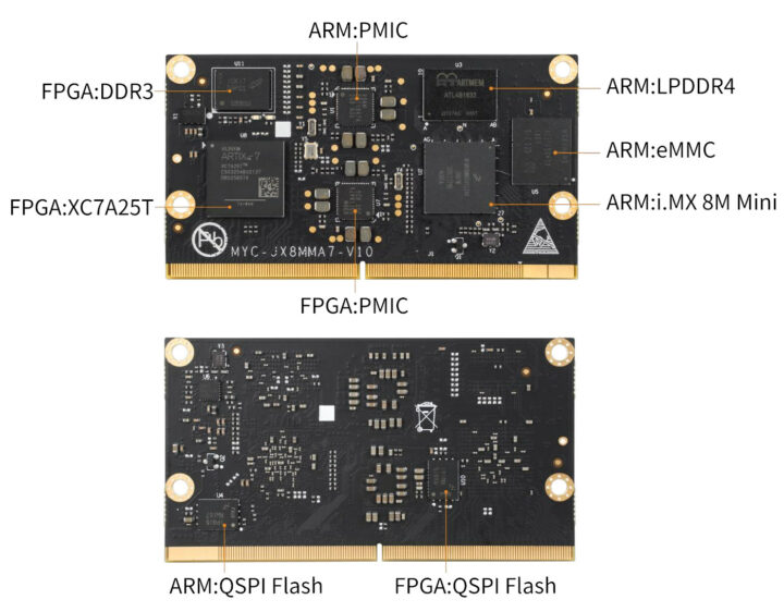
The 82 x 45mm CPU module comes with 2GB LPDDR4, 8GB eMMC flash, and 32MB QSPI Flash for the Arm processor and 256MB DDR3 and 32MB QSPI Flash for FPGA. It exposes I/Os through an MXM 3.0 edge connector and can operate in the industrial temperature range (-40 to 85°C).
MYC-JX8MMA7 CPU module specifications:
- SoC – NXP i.MX 8M Mini with quad-core Cortex-A53 processor @ up to 1.6 (industrial) or 1.8 GHz, Cortex-M4F real-time core @ 400 MHz, Vivante GC320 and Vivante GCNanoUltra 3D/2D GPUs, 1080p60 H.265, H.264, VP8, VP9 video decoder, 1080p60 H.264 & VP8 video encoder
- FPGA – AMD Xilinx Artix-7 XC7A25T-2CSG325 with 23,360 logic cells, 3x GTP
- System Memory and Storage
- SoC – 2GB LPDDR4, 8GB eMMC flash, and 32MB QSPI Flash
- FPGA – 256MB DDR3 and 32MB QSPI Flash
- 314-pin MXM 3.0 edge connector with
- CPU subsystem
- Display – 1x MIPI DSI
- Camera – 1x MIPI CSI
- Audio – 8-ch PDM input, 3x SAI/I2S
- Networking – Gigabit Ethernet with IEEE 1588 and AVB support
- USB – 2x USB 2.0 interfaces
- 1x PCIe 2.0
- 2x SDIO
- Low-speed I/Os – 3x SPI, 4x I2C, 4x UART
- FPGA subsystem
- 3x GTP
- 105x HR I/O
- 1x JTAG
- CPU subsystem
- 2x Power Management IC (BD71847AMWV) one of the NXP processor, the other for the Xilinx FPGA
- Dimensions – 82 x 45 mm
- Junction Temperature Range
- Commercial – 0 to 90°C
- Industrial – -40 to 105°C

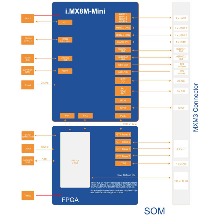
Based on the block diagram above, the FPGA and CPU are interfaced via PCIe x1, I2C, and interrupts.
MYiR provides two Yocto-built Linux images based on Linux 5.10.72 and U-boot 2021.04 and all drivers for peripherals, one with Qt, and the other without. There’s no mention of specific software or sample code for the Artix-7 FPGA, so you’d probably be expected to use Xilinx tools like the ISE Design Suite.
The company already provides Arm+FPGA through modules based on AMD Xilinx Zynq-7000 or Zynq Ultrascale+ FPGA SoCs, and the main reason I can see for doing a two-chip solution is improved multimedia capabilities with a more modern GPU and a built-in VPU for video encoding/decoding. But there must be other that I am missing.
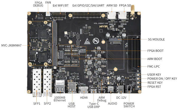
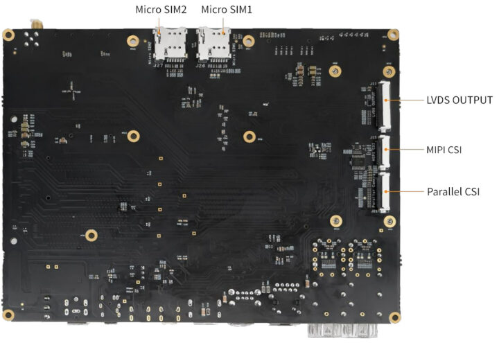
The MYD-JX8MMA7 development board enables users to test the features of the CPU module with two SFP cages, one Gigabit Ethernet RJ45 port, HDMI and LVDS video interfaces, MIPI CSI and parelle camera interfaces, USB ports, an audio jack, two microSD card slots (one for the Arm CPU, the other for the FPGA), an FMC-LPC connector, and various headers. There’s a socket for a 5G module accompanied by two micro SIM card sockets.
MYiR sells the commercial-grade CPU Module for $109, and the industrial variant for $119.The related development boards with accessories such as a 12V/2A power supply sell for $199 and $219 respectively. More details and purchased links can be found on the product page.

Jean-Luc started CNX Software in 2010 as a part-time endeavor, before quitting his job as a software engineering manager, and starting to write daily news, and reviews full time later in 2011.
Support CNX Software! Donate via cryptocurrencies, become a Patron on Patreon, or purchase goods on Amazon or Aliexpress. We also use affiliate links in articles to earn commissions if you make a purchase after clicking on those links.


… what’s the advantage over the Kria modules?
much cheaper
A stand out feature, the FPGA has its own DDR3 memory. So, the FPGA processing will not impact the ARM53/M4 cores. Maybe this will be used for some type of off loading image processing?