
Intel introduced high-end Alder Lake Hybrid processor family for consumer devices a couple of months ago, with Pentium G7400 and Celeron G6900 leaking a few weeks later, and now the company has formally announced the Alder Lake-S and Alder Lake-H processor families for respectively desktop IoT and mobile IoT solutions, as well as more efficient U-series and P-series of 12th Gen Intel Core Alder Lake IoT processors with a TDP ranging from 15W to 28W.
Alder Lake S-Series desktop processors for IoT
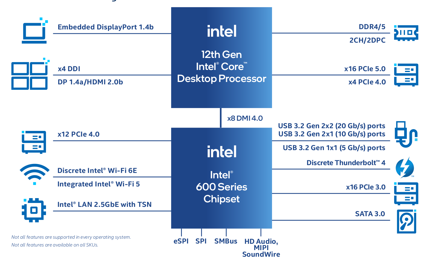 Key features and specifications:
- CPU
- Up to 16 cores, up to 24 threads in IoT SKUs
- Up to 30 MB Intel Smart Cache
- TDP – 35W to 65W
- Real-time capability on select SKUs
- Graphics/Video
- Intel UHD Graphics 770 driven by Intel Xe architecture with up to 32 EUs
- Up to four independent displays up to 4K or one display at 8K resolution
- Up to two video decode boxes (VDboxes)
- AI Accelerators – Intel DL Boost with VNNI instructions on the CPU, int8/dp4 instructions on the GPU
- Memory – Up to 64GB DDR5-4800 or DDR4-3200 RAM
- Storage – SATA 3.0, PCIe
- Networking
- Discrete 2.5GbE LAN
- Integrated Intel Wi-Fi 5 (802.11ac) and support for discrete Intel Wi-Fi 6E with embedded-use conditions
- USB – Discrete Thunderbolt 4 or USB4, multiple USB 3.2 Gen 2×2 (20 Gbps), USB 3.2 Gen 2×1 (10 Gbps)
- PCIe
- Up to 16 lanes PCIe 5.0, up to four lanes PCIe 4.0 on the CPU
- Up to 12 lanes PCIe 4.0, up to 16 lanes PCIe 3.0 on the PCH
- Security and manageability
- Intel vPro platform eligible on select SKUs
- Intel Converged Security and Management Engine version 16
- LGA socket
- Intel 7 process technology
On the software side, the processors support Windows 10 IoT Enterprise 2021 LTSC, Yocto Project Linux, community-supported Celadon (Android) in VM, and Wind River VxWorks 7 operating systems, as well as KVM and ACRN hypervisors, plus UEFI and Slim Bootloader firmware.
There’s now a fairly long list of Core-i3 to Core-i9 from the Alder Lake Desktop family.
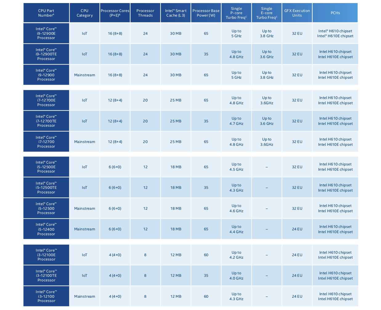
It should be noted on Core-i7 and Core-i9 parts are actual hybrid processors, with the Core-i3 and Core-i5 SKUs missing the efficient cores, which would provide less power saving due to the lower performance cores’ frequency and add to the costs. The table above taken from the product brief does not include the Pentium and Celeron part, but the product page does, and those are the embedded versions of leaked parts we mentioned in the introduction with Pentium G7400E/TE and Celeron G6900E/TE.
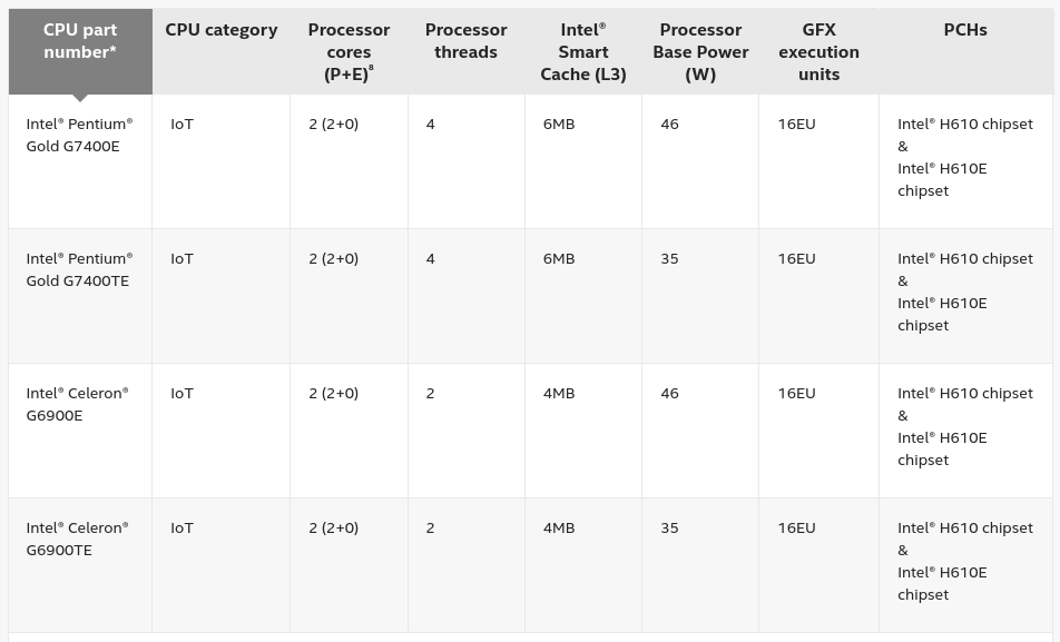
The Pentium parts are dual-core,four-thread processors, while the Celeron processor comes with two cores as well, but no multi-threading.
Intel says the Alder Lake S-Series processors deliver up to 1.36 times faster single-thread performance, up to 1.35 times faster multithreaded performance, up to 1.94x faster graphics performance, and up to 2.81x faster “in GPU image classification inference performance compared to equivalent 10th generation Intel Core processors.
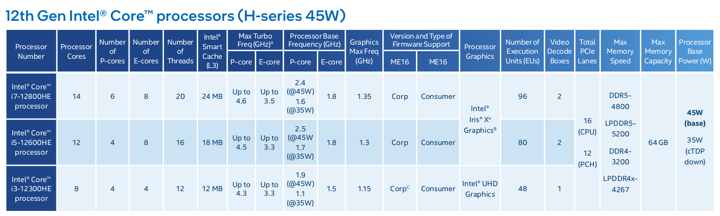
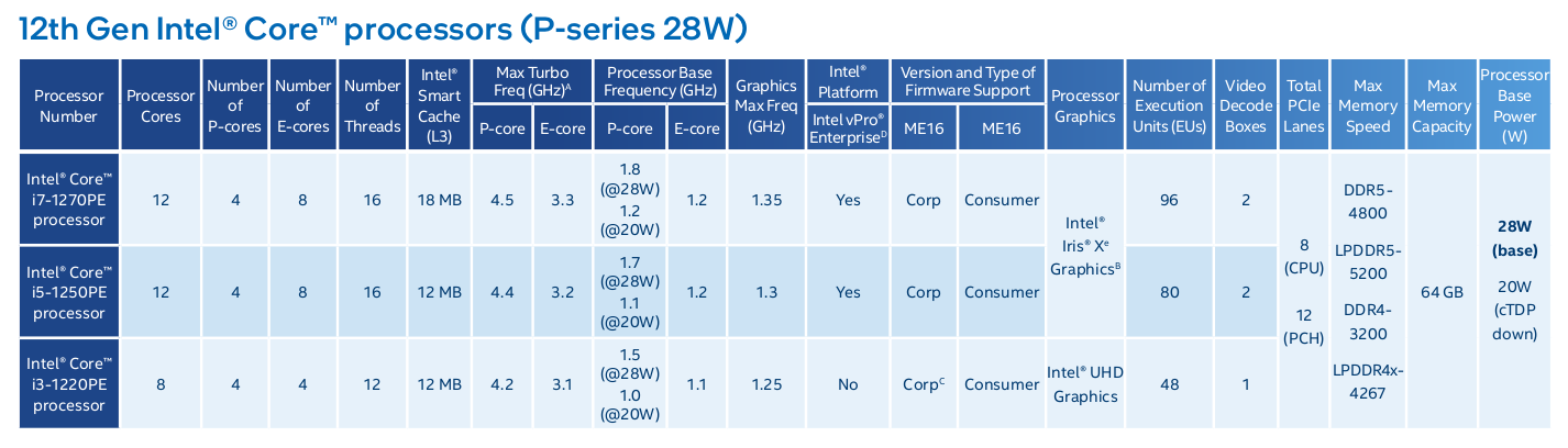
Alder Lake H-series, U-Series, and P-Series IoT processors
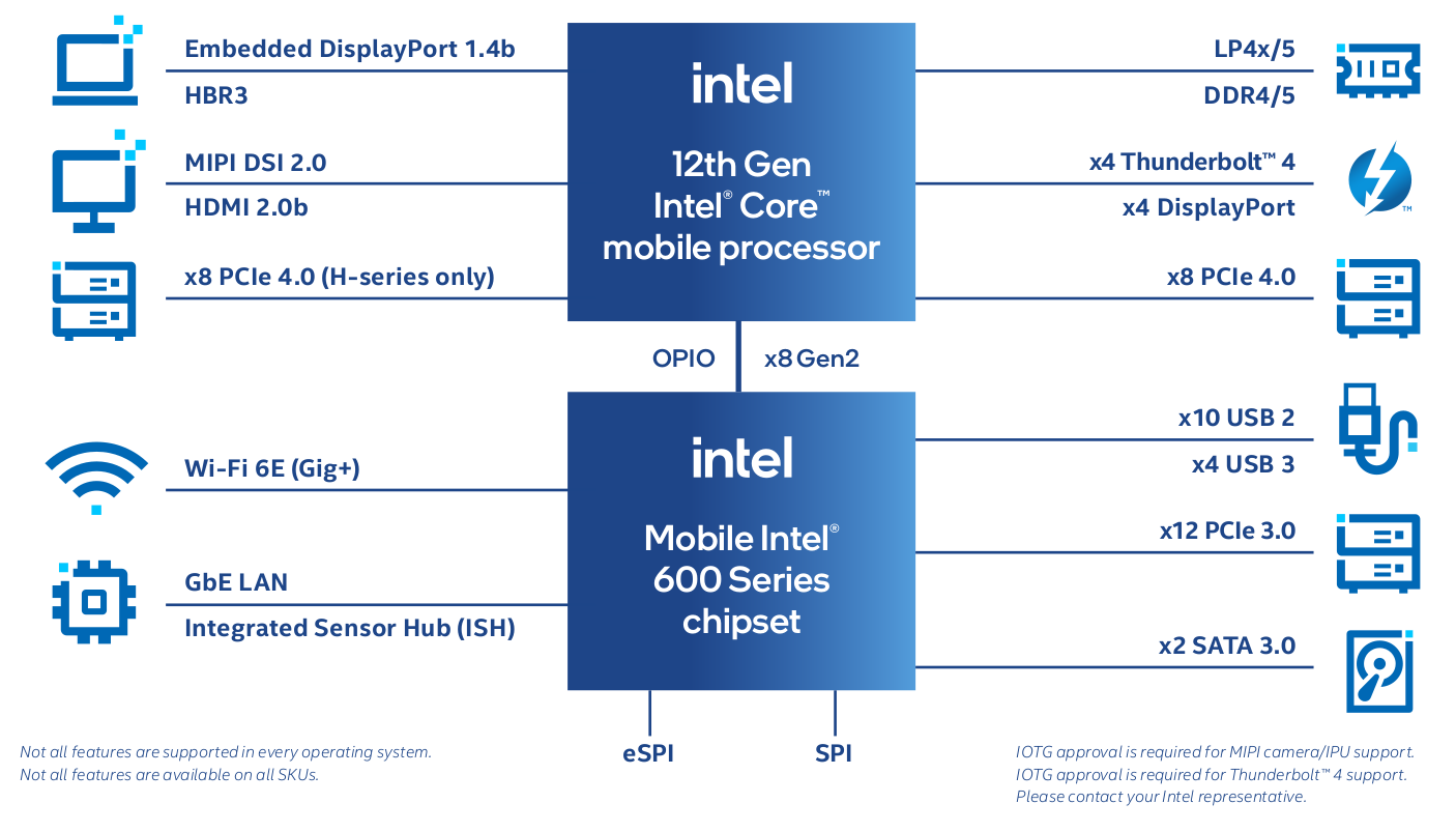 Key features and specifications:
- CPU
- Up to 14 cores, up to 20 threads in IoT SKUs
- Up to 24 MB Intel Smart Cache
- TDP – 15W to 45W
- Graphics/Video
- Intel Xe graphics with up to 96 EUs
- HDMI 2.1 with LPSPON
- Up to four independent displays up to 4Kp60 HDR or one display at 8K resolution
- Up to two video decode boxes (VDboxes)
- AI Accelerators – Intel DL Boost with VNNI instructions on the CPU, DP4a instructions on the GPU
- Memory – Up to 64GB DDR5-4800, LP5-5200, DDR4-3200, LP4x-4267 RAM
- Storage – 2x SATA 3.0, PCIe
- Networking
- Integrated Gigabit Ethernet port, 2.5GbE discrete LAN
- Integrated Intel Wi-Fi 5 (802.11ac)/Bluetooth 5.1 (Wireless-AC 9560) and support for discrete Intel Wi-Fi 6E/Bluetooth 5.2 (AX210) with embedded-use conditions
- Intel 5G platform based on Intel’s host modem SW and M.2 module from Fibocom
- USB – Discrete Thunderbolt 4 or USB4, multiple USB 3.2 Gen 2×2 (20 Gbps), USB 3.2 Gen 2×1 (10 Gbps)
- PCIe
- Up to 16 lanes PCIe 4.0 on the CPU
- Up to 12 lanes PCIe 3.0 on the PCH
- Security and manageability
- Intel vPro platform eligible on select SKUs
- Intel Converged Security and Management Engine version 16
- BGA package
- Intel 7 process technology
Software support is the same as for the Alder Lake S-series desktop IoT processors, but we have more manageable lists of parts for all three H-Series, P-Series, and U-Series processors, and all of those are hybrid SoCs for Performance and Efficient cores.
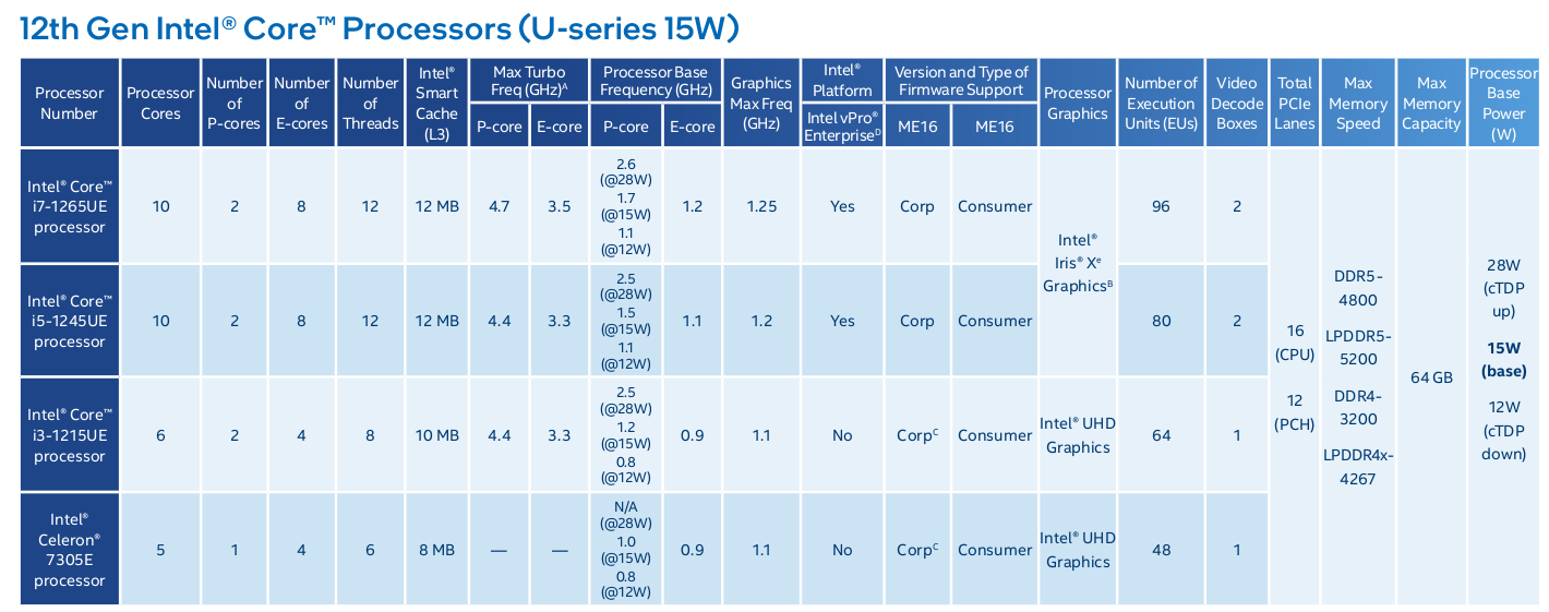
The 15W Alder Lake U-Series may be quite interesting for single board computers and mini PCs providing those IoT SKUs are not too expensive. The Intel Celeron 7305E penta-core processor comes with one performance core @ 1.0 GHz, four efficient cores @ 0.9 GHz, as well as a 48EU Intel UDH graphics clocked at up to 1.1 GHz. No max turbo speeds are listed for the part, which I find odd, as a 1 GHz processor without turbo boost would be quite slow, even when taking into account architectural improvements.
Intel compares the Mobile IoT parts to equivalent 11th gen IoT processors with claims of 1.04x and 1.18x faster single-thread/multi-thread performance, and up to 2.29x faster graphics performance. So maybe we should not expect a massive performance increase over Tiger Lake processors, except for graphics. More details may be found on the product page.
The new Alder Lake IoT processor will be found in a wide range of products including retail PoS, digital signage, medical imaging equipment, computer-vision enhanced factory equipment, and network video recorders (NVRs) with built-in video analytics.

Jean-Luc started CNX Software in 2010 as a part-time endeavor, before quitting his job as a software engineering manager, and starting to write daily news, and reviews full time later in 2011.
Support CNX Software! Donate via cryptocurrencies, become a Patron on Patreon, or purchase goods on Amazon or Aliexpress. We also use affiliate links in articles to earn commissions if you make a purchase after clicking on those links.


65W – IOT – really ?
I think they’ve broadened the meaning of IoT a bit…
Now digital signage, a visual inspection machine at the factory, medical imaging equipment are all “IoT”.
I find it particularly shocking to read 35 or 46W for G6900E/TE for only 2 cores and 2 threads with only 4MB cache! Sounds like we’re progressively regressing down to the Pentium4!
Well, these two new Celerons don’t support Burst/Turbo mode but their Base Frequency is listed as 2.4 GHz (35W PBP) and 3.0 GHz (46W PBP)… which is what has been called in the past ‘Burst Frequency’.
Older Jasper Lake Celerons were able to ‘burst’ while the announced TDP talked about something entirely differently. The 2C/2T Celeron N4500 is advertised with a 6W TDP (full load at a Base Frequency of 1.1GHz) while the power draw at 2.8 GHz is an entirely different and especially untold story.
So we’re comparing 2C/2T at 3.0 GHz / 46W with 2.8 GHz capable 2C/2T at 1.1 GHz / 6W since it’s just replacing one BS metric with another: Processor Base Power (PBP) vs. TDP.
PBP is defined as ‘The time-averaged power dissipation that the processor is validated to not exceed during manufacturing while executing an Intel-specified high complexity workload at Base Frequency and at the junction temperature as specified in the Datasheet for the SKU segment and configuration.’
Who knows which engines this ‘Intel-specified high complexity workload’ uses? Only CPU? GPGPU / AI Accelerators also? QuickSync stuff too?
Interesting! I had not noticed they changed the metric for power dissipation…
TDP definition:
PBP definition (already in your comment, but I had it here again for easier comparison)
It looks pretty similar to me except they added working about the junction temperature.
There’s an interview of an Intel engineer on AnandTech about TDP measurements and the “high complexity workload”:
> TDP vs. PBP … It looks pretty similar to me
For me not since with TDP Intel talks about ‘with all cores active’ while ‘cores’ are gone with the PBP definition so the latter workload might include stuff that happens away from the CPU cores (GPGPU, AI acceleration on both CPU and GPU, video and even 2D/3D acceleration stuff)
The PBP to me seems more like a real upper consumption limit while the TDP became just plain BS recently.
OK but still. 2 cores at 2.4GHz for 35W… I mean, that’s the expected consumption of my LX2160A with 16 cores at 2.2 GHz! And that doesn’t deliver the same performance at all! Also the J4105 on one of my dev boards runs 4 cores at 2.4 GHz entirely fanless with a small heat sink so it’s closer to 10W than 35W.
> 2 cores at 2.4GHz for 35W
You’re still talking about ‘CPU cores only active’ which excludes most real-world workloads by today’s standards since a long time. These Celerons come with two ‘performance’ CPU cores, an UHD 710 IGP with 16 EU at up to 1.3GHz, a DMI attached PCH, 20 PCIe Gen4 lanes, ‘Gaussian & Neural Accelerator’, ‘Deep Learning Boost’ and whatever else.
Which of these ‘engines’ being fully loaded is icluded in the PBP number?
> J4105
Just checked, the Alder Lake Celerons seem to be the first with state of the art Intel Vector Extensions. In the past they always missed them (at least Jasper Lake is still limited to SSE4.2). But I’ve no idea what this means consumption wise…
Anyway: with your ‘build farm’ use case I would expect better power efficiency compared to this Gemini Lake thingy since most CPU ‘engines’ being in deep sleep all the time with such ‘CPU only’ workloads.
Note I’m not specifically speaking about a build farm or such a thing, just as a user buying a motherboard, once which can be fanless for all use cases and the other definitely not based on the advertised numbers. Even if for *my* use cases it turns out it doesn’t heat that much, it will not be built fanless by the board vendor just because it could happen to be insufficient for some other use cases.
> the advertised numbers
Again: do you know what the PBP workload includes? Me not.
Intel’s TDP has become a joke (see this Anandtech testing where the 65W i7-10700 draws 215W while the 125W rated i7-10700K limits itself to 205W).
So maybe the PBP is a more honest number really representing the maximum power draw of the ‘whole CPU’ which unlike those older Gemini Lake thingies is not just a SoC any more but a combination of CPU and PCH interconnected by multiple DMI lanes which alone need some juice. Then there is a bunch of stuff that simply didn’t exist with Gemini Lake or is now much more powerful.
And if these high PBP numbers don’t allow any board maker to go with fanless designs then be it that way.
I’m still happy with a less capable Jasper Lake Celeron in a tiny fanless box idling at 2.7W (19V power brick included) and now serving as a Check_MK host monitoring thousands of services at around 6W. But I would expect similar or lower power draw with a carefully designed G6900E/TE box with same workload.
> Again: do you know what the PBP workload includes? Me not.
For me PBP is the CPU guarantees never to go beyond at the base frequency, so the workload is not quite relevant, it is expected to be the worst possible one ever (i.e. a dream program for stress-ng). These should be programs which involve many “expensive” instructions that typically result in the time spent in PL2 to quickly be exhausted. That doesn’t change the fact that in order to stand such a workload for a while, adequate cooling is needed to cover the PBP. And you’re not forbidden from running them on older fanless CPUs whose extremely low TDP is exploded in this case but remains OK for a lone heat sink.
Most probably we’re still talking past each other 🙂
I’m assuming PBP not just being CPU cores but also including other IP blocks.
There’s an i5-12500E with 3 times more performance cores, twice the EU at a similar Base Frequency like the G6900E. And the i5-12500E has a 65W PBP rating while the Celeron is at 46W. Even if those dual core Celerons are pure garbage and need insanely high voltages this difference shouldn’t be possible if it’s only about CPU workloads.
> I’m assuming PBP not just being CPU cores but also including other IP blocks.
Ah OK that’s the point I didn’t get from your explanation. Yes maybe they’re using that to justify this insane difference.
So at the low end, which we would likely see in small mini PC’s and SBC’s, still stuck on UHD graphics, where Iris should be the default.
It’s no wonder that Arm is due to catch up with them very soon Intel continues to kick itself towards eventual extinction.
Why oversell your IP and start a arms race where none is needed. Intel have enough of a fight with AMD and Apple.